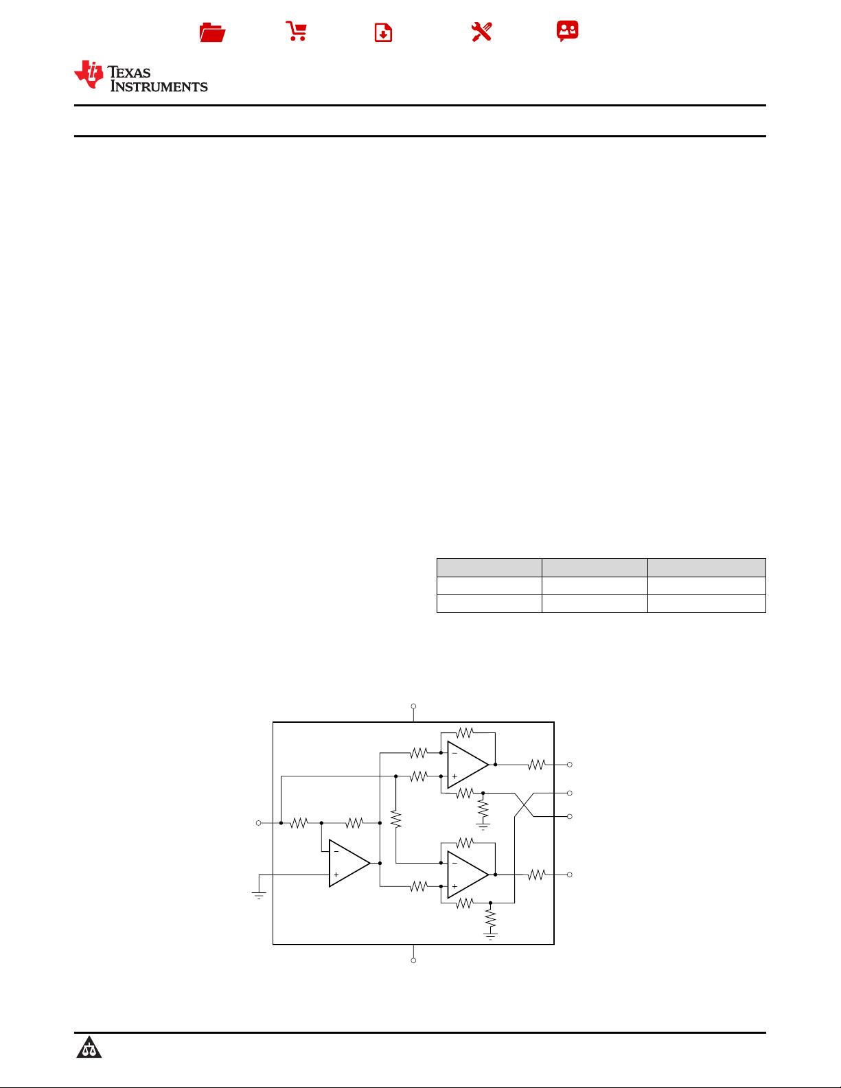
没有合适的资源?快使用搜索试试~ 我知道了~
TI-DRV135.pdf
需积分: 5 0 下载量 124 浏览量
2022-12-03
23:52:03
上传
评论 4
收藏 1.91MB PDF 举报
温馨提示
试读
33页
TI-DRV135.pdf
资源详情
资源评论
V
IN
Gnd
+V
O
A2
10kΩ
50Ω
50Ω
All resistors 30kΩ unless otherwise indicated.
V+
+Sense
–Sense
–V
O
V–
A3
A1
10kΩ
Product
Folder
Sample &
Buy
Technical
Documents
Tools &
Software
Support &
Community
DRV134
,
DRV135
SBOS094B –JANUARY 1998–REVISED DECEMBER 2014
DRV13x Audio-Balanced Line Drivers
1 Features 3 Description
The DRV134 and DRV135 are differential output
1
• Balanced Output
amplifiers that convert a single-ended input to a
• Low Distortion: 0.0005% at f = 1 kHz
balanced output pair. These balanced audio drivers
• Wide Output Swing: 17Vrms into 600 Ω
consist of high performance op amps with on-chip
precision resistors. They are fully specified for high
• High Capacitive Load Drive
performance audio applications and have excellent ac
• High Slew Rate: 15 V/µs
specifications, including low distortion (0.0005% at 1
• Wide Supply Range: ±4.5 V to ±18 V
kHz) and high slew rate (15 V/µs).
• Low Quiescent Current: ±5.2 mA
The on-chip resistors are laser-trimmed for accurate
• 8-Pin DIP, SO-8, and SOL-16 Packages
gain and optimum output common-mode rejection.
Wide output voltage swing and high output drive
• Companion to Audio Differential Line Receivers:
capability allow use in a wide variety of demanding
INA134 and INA137
applications. They easily drive the large capacitive
• Improved Replacement for SSM2142
loads associated with long audio cables. Used in
combination with the INA134 or INA137 differential
2 Applications
receivers, they offer a complete solution for
transmitting analog audio signals without degradation.
• Audio Differential Line Drivers
• Audio Mix Consoles
The DRV134 is available in 8-pin DIP and SOL-16
surface-mount packages. The DRV135 comes in a
• Distribution Amplifiers
space-saving SO-8 surface-mount package. Both are
• Graphic and Parametric Equalizers
specified for operation over the extended industrial
• Dynamic Range Processors
temperature range, –40°C to +85°C and operate from
–55°C to +125°C.
• Digital Effects Processors
• Telecom Systems
Device Information
(1)
• Hi-Fi Equipment
PART NUMBER PACKAGE BODY SIZE (NOM)
• Industrial Instrumentation
DRV134 SOIC (16) 10.30 mm × 7.50 mm
DRV135 SOIC (8) 4.90 mm × 3.91 mm
(1) For all available packages, see the orderable addendum at
the end of the datasheet.
4 Simplified Schematic
1
An IMPORTANT NOTICE at the end of this data sheet addresses availability, warranty, changes, use in safety-critical applications,
intellectual property matters and other important disclaimers. PRODUCTION DATA.
DRV134
,
DRV135
SBOS094B –JANUARY 1998–REVISED DECEMBER 2014
www.ti.com
Table of Contents
8.4 Device Functional Modes........................................ 13
1 Features.................................................................. 1
9 Application and Implementation ........................ 15
2 Applications ........................................................... 1
9.1 Application Information............................................ 15
3 Description ............................................................. 1
9.2 Typical Application ................................................. 15
4 Simplified Schematic............................................. 1
10 Power Supply Recommendations ..................... 17
5 Revision History..................................................... 2
11 Layout................................................................... 17
6 Pin Configuration and Functions......................... 3
11.1 Layout Guidelines ................................................. 17
7 Specifications......................................................... 4
11.2 Layout Examples................................................... 18
7.1 Absolute Maximum Ratings ...................................... 4
11.3 Thermal Performance ........................................... 19
7.2 Handling Ratings....................................................... 4
12 Device and Documentation Support ................. 19
7.3 Recommended Operating Conditions ...................... 4
12.1 Documentation Support ........................................ 19
7.4 Electrical Characteristics........................................... 5
12.2 Related Links ........................................................ 19
7.5 Typical Characteristics.............................................. 6
12.3 Trademarks........................................................... 19
8 Detailed Description............................................ 11
12.4 Electrostatic Discharge Caution............................ 19
8.1 Overview ................................................................. 11
12.5 Glossary................................................................ 19
8.2 Functional Block Diagram ....................................... 11
13 Mechanical, Packaging, and Orderable
8.3 Feature Description................................................. 11
Information ........................................................... 20
5 Revision History
Changes from Revision A (April 2007) to Revision B Page
• Added Handling Rating table, Feature Description section, Device Functional Modes, Application and
Implementation section, Power Supply Recommendations section, Layout section, Device and Documentation
Support section, and Mechanical, Packaging, and Orderable Information section ............................................................... 1
2 Submit Documentation Feedback Copyright © 1998–2014, Texas Instruments Incorporated
Product Folder Links: DRV134 DRV135
Top View 8-Pin DIP/SO-8
Top View SOL-16
1
2
3
4
5
6
7
8
16
15
14
13
12
11
10
9
NC
NC
+V
O
+Sense
V+
V–
NC
NC
NC
NC
–V
O
–Sense
Gnd
V
IN
NC
NC
1
2
3
4
8
7
6
5
+V
O
+Sense
V+
V–
–V
O
–Sense
Gnd
V
IN
DRV134
,
DRV135
www.ti.com
SBOS094B –JANUARY 1998–REVISED DECEMBER 2014
6 Pin Configuration and Functions
NOTE: NC - No internal connection
Pin Functions
PIN
I/O DESCRIPTION
NAME DIP-8 and SO-8 SOL-16
Gnd 3 5 – Ground
+Sense 7 13 I Sensing, non-inverting input
–Sense 2 4 I Sensing, inverting input
V+ 6 12 – Positive supply
V– 5 11 – Negative supply
V
IN
4 6 I Input
–V
o
1 3 O Inverted, balanced differential output
+V
o
8 14 O Balanced differential output
NC – 1,2,7,8,9,10,15,16 – These pins should be left unconnected
Copyright © 1998–2014, Texas Instruments Incorporated Submit Documentation Feedback 3
Product Folder Links: DRV134 DRV135
DRV134
,
DRV135
SBOS094B –JANUARY 1998–REVISED DECEMBER 2014
www.ti.com
7 Specifications
7.1 Absolute Maximum Ratings
over operating free-air temperature range (unless otherwise noted)
(1)
MIN MAX UNIT
Supply voltage, V+ to V– 40 V
Input voltage range V– V+
Output short-circuit (to ground) Continuous
Operating temperature –55 125 °C
Junction temperature 150 °C
(1) Stresses beyond those listed under Absolute Maximum Ratings may cause permanent damage to the device. These are stress ratings
only, which do not imply functional operation of the device at these or any other conditions beyond those indicated under Recommended
Operating Conditions . Exposure to absolute-maximum-rated conditions for extended periods may affect device reliability.
7.2 Handling Ratings
MIN MAX UNIT
T
stg
Storage temperature range –55 125 °C
Human body model (HBM), per ANSI/ESDA/JEDEC JS-001, all –2000 2000
pins
(1)
V
(ESD)
Electrostatic discharge V
Charged device model (CDM), per JEDEC specification –500 500
JESD22-C101, all pins
(2)
(1) JEDEC document JEP155 states that 500-V HBM allows safe manufacturing with a standard ESD control process.
(2) JEDEC document JEP157 states that 250-V CDM allows safe manufacturing with a standard ESD control process.
7.3 Recommended Operating Conditions
over operating free-air temperature range (unless otherwise noted)
MIN NOM MAX UNIT
T
spe
Specification temperature range –40 85 °C
T
A
Operation temperature range –55 125 °C
V+ Positive supply 4.5 18 18 V
V– Negative supply –4.5 –18 –18 V
4 Submit Documentation Feedback Copyright © 1998–2014, Texas Instruments Incorporated
Product Folder Links: DRV134 DRV135
DRV134
,
DRV135
www.ti.com
SBOS094B –JANUARY 1998–REVISED DECEMBER 2014
7.4 Electrical Characteristics
At T
A
= +25°C, V
S
= ±18 V, R
L
= 600 Ω differential connected between +V
O
and –V
O
, unless otherwise noted.
PARAMETER TEST CONDITIONS MIN TYP MAX UNIT
AUDIO PERFORMANCE
THD+N Total Harmonic Distortion + Noise 0.001%
f = 20Hz to 20kHz, V
O
= 10Vrms
0.0005%
f = 1kHz, V
O
= 10Vrms
20 kHz BW
RTO
(1)
Noise Floor –98 dBu
THD+N < 1%
RTO
(1)
Headroom 27 dBu
INPUT
Z
IN
Input Impedance
(2)
10 kΩ
I
IN
Input Current V
IN
= ±7.07 V –1000 ±700 1000 µA
GAIN
Differential
Initial 5.8 6 dB
[(+V
O
) – (–V
O
)]/V
IN
V
IN
= ±10V
Error –2% ±0.1% 2%
Error vs Temperature ±10 ppm/°C
Single-Ended V
IN
= ±5V
Initial 5.8 6 dB
Error –2% ±0.7% 2%
Error vs Temperature ±10 ppm/°C
Nonlinearity 0.0003 % of FS
OUTPUT
OCMR Common-Mode Rejection, f = 1kHz See Figure 25 46 68 dB
SBR Signal Balance Ratio, f = 1kHz See Figure 26 35 54 dB
Output Offset Voltage
V
OCM
(3)
Offset Voltage, Common-Mode V
IN
= 0 –250 ±50 250 mV
Offset Voltage, Common-Mode vs ±150 µV/°C
Temperature
V
OD
(4)
Offset Voltage, Differential V
IN
= 0 –10 ±1 10 mV
Offset Voltage, Differential vs Temperature ±5 µV/°C
PSRR Offset Voltage, Differential vs Power Supply V
S
= ±4.5V to ±18V 80 110 dB
Positive (V+) – 3 (V+) – 2.5
Output Voltage Swing, No Load
(5)
V
Negative (V–) + 2 (V–) + 1.5
Impedance 50 Ω
C
L
Load Capacitance, Stable Operation C
L
Tied to Ground (each output) 1 µF
I
SC
Short-Circuit Current ±85 mA
FREQUENCY RESPONSE
Small-Signal Bandwidth 1.5 MHz
SR Slew Rate 15 V/µs
Settling Time: 0.01% V
OUT
= 10V Step 2.5 µs
Overload Recovery Output Overdriven 10% 3 µs
POWER SUPPLY
V
S
Rated Voltage ±18 V
Voltage Range ±4.5 ±18 V
I
Q
Quiescent Current I
O
= 0 –5.5 ±5.2 5.5 mA
(1) dBu = 20log (Vrms /0.7746); RTO = Referred-to-Output.
(2) Resistors are ratio matched but have ±20% absolute value.
(3) V
OCM
= [(+V
O
) + (–V
O
)] / 2.
(4) V
OD
= (+V
O
) – (–V
O
).
(5) Ensures linear operation. Includes common-mode offset.
Copyright © 1998–2014, Texas Instruments Incorporated Submit Documentation Feedback 5
Product Folder Links: DRV134 DRV135
剩余32页未读,继续阅读
安全验证
文档复制为VIP权益,开通VIP直接复制
信息提交成功
评论0
最新资源