TI-HD3SS212.pdf
需积分: 5 36 浏览量
2022-12-01
23:45:32
上传
评论 4
收藏 1.21MB PDF 举报

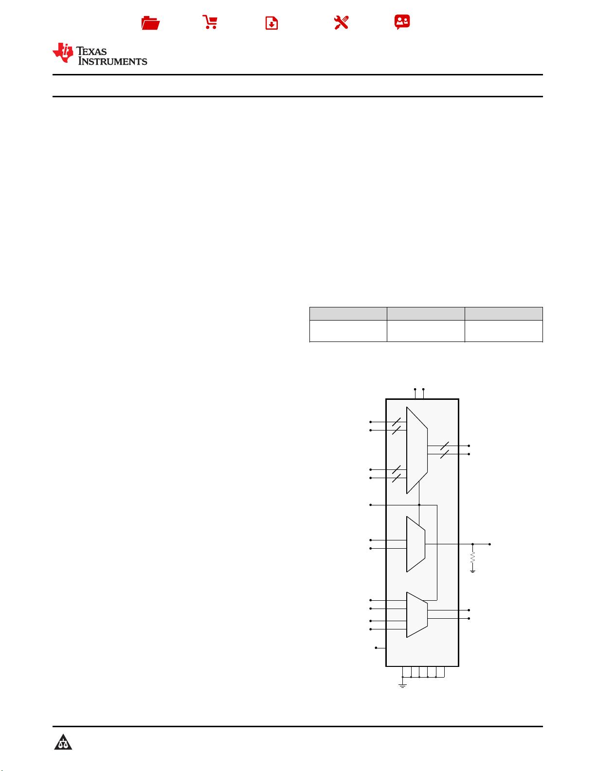
Dx_SEL
HPDA
HPDB
VDD
OE
GND
AUXA (p)
AUXA (n)
AUXB (p)
AUXB (n)
DAz (p)
DAz (n)
DBz(p)
DBz(n)
SEL
SEL
SEL
HD3SS212
SEL = 0
SEL = 1
4
4
4
4
4
4
(z = 0,1, 2or3)
HPDC
DCz
(p)
DCz
(n)
AUXC
(p)
AUXC
(n)
SEL = 1
SEL = 0
SEL = 1
SEL = 0
125kW
Product
Folder
Sample &
Buy
Technical
Documents
Tools &
Software
Support &
Community
An IMPORTANT NOTICE at the end of this data sheet addresses availability, warranty, changes, use in safety-critical applications,
intellectual property matters and other important disclaimers. PRODUCTION DATA.
English Data Sheet: SLAS822
HD3SS212
ZHCS600C –DECEMBER 2011 –REVISED OCTOBER 2016
HD3SS212 5.4Gbps DisplayPort 1.2 2 选选 1 差差动动开开关关
1
1 特特性性
1
• 与Displayport 1.2的电气标准兼容
• 2:1开关支持的最高数据速率为5.4Gbps
• 支持热插拔检测(HPD)开关
• 在5.4 GHz上宽-3dB差分带宽(BW)
• 出色的动态特性(2.7GHz情况下)
– 串扰 = -50dB
– 隔音 = -22dB
– 插入损耗 = –1.4dB
– 回波损耗 = –11dB
– 最大位到位失真 = 4ps
• 漏极电源电压电压(VDD)运行范围3.3V ± 10%
• 小型 5mm x 5mm x 1mm,48 焊球 u*BGA 封装方
式
• 输出使能 (OE) 引脚禁用开关以省电
• 功耗
– HD3SS212 < 10mW(待机功耗 < 30µW,此
时,OE = L)在整个文档内将
2 应应用用
• 需要 DP 和 PCI Express 的 主板 应用
• 台式电脑
• 笔记本电脑
• 底座
3 说说明明
HD3SS212 是一款高速无源开关,能够在应用中将两
个完全 DisplayPort 4 通道端口从两个源之一切换到一
个目标位置。对于 DisplayPort 应用, HD3SS212 还
支持在辅助 (AUX) 和热插拔检测 (HPD) 信号间切换。
HPD 路径是一个缓冲器,此缓冲器在 HPDC 线路上要
求一个 125kΩ 下拉电阻。
一个典型应用将是包含 2 个图形处理单元 (GPU) 的主
板,这些处理单元需要驱动一个 DisplayPort 负输出。
GPU 由 Dx_SEL 引脚选择。HD3SS212 采用 48 焊球
球状引脚栅格阵列 (BGA) 封装方式并在 -40°C 至
105°C 的完全工业温度范围内由 3.3V 单电源供电运
行。
器器件件信信息息
(1)
器器件件型型号号 封封装装 封封装装尺尺寸寸((标标称称值值))
HD3SS212
BGA MicroStar
Junior (48)
5.00mm x 5.00mm
(1) 要了解所有可用封装,请见数据表末尾的可订购产品附录。
功功能能方方框框图图
剩余23页未读,继续阅读
资源评论


