没有合适的资源?快使用搜索试试~ 我知道了~
资源推荐
资源详情
资源评论


VCONN
Channel
Configuration
Mode
Configuration
and Detection
CC1
VDD5
ControllerI2C GPIOs
TX2
RX2
TX1
RX1
TX
RX
CC2
VBUS_DET
VBUS
Detection
USB
SS
Mux
Copyright © 2016, Texas Instruments Incorporated
Product
Folder
Sample &
Buy
Technical
Documents
Tools &
Software
Support &
Community
An IMPORTANT NOTICE at the end of this data sheet addresses availability, warranty, changes, use in safety-critical applications,
intellectual property matters and other important disclaimers. PRODUCTION DATA.
English Data Sheet: SLLSES1
HD3SS3220
ZHCSFC4A –DECEMBER 2015–REVISED AUGUST 2016
HD3SS3220 具具有有超超高高速速 2:1 MUX 的的 USB Type-C DRP 端端口口控控制制器器
1
1 特特性性
1
• 集成了 2:1 超高速 Mux 的 USB Type-C 端口控制
器
• 兼容 USB Type-C™ 规格
• 支持高达 10Gbps 的 USB 3.1 G1 和 G2
• 支持高达 15W 的功率输出与 3A 的电流通告和检测
• 模式配置
– 仅主机 - 下行端口 (DFP)/仅
– 源设备 – 上行端口 (UFP)/接收设备
– 双角色端口 – DRP
• 通道配置 (CC)
– USB 端口连接检测
– 电缆方向检测
– 角色检测
– Type-C 电流模式(默认、中等和高)
• 对于有源电缆的 V
(BUS)
检测和 VCONN 支持
• 音频和调试附件支持
• 支持 Try.SRC 和 Try.SNK DRP 模式
• 通过通用输入/输出 (GPIO) 和 I
2
C 控制配置
• 工作和待机电流消耗都很低
• 工业温度范围:–40°C 至 85°C
2 应应用用
• USB 主机、设备、集线器
• 移动电话、平板电脑和笔记本
• U 盘、移动硬盘、机顶盒等 USB 外设
3 说说明明
HD3SS3220 是一款具有 DRP 端口控制器的 USB 超
高速 (SS) 2:1 多路复用器。该器件可为生态系统实现
USB Type-C 提供通道配置 (CC) 逻辑和 5V VCONN
电源。HD3SS3220 可配置为下行端口 (DFP)、上行端
口 (UFP) 或双角色端口 (DRP),因此成为任何应用的
理想之选。
根据 Type-C 规范,HD3SS3220 在 DRP 模式下会交
替将自身配置为 DFP 或 UFP。CC 逻辑块通过监视
CC1 和 CC2 引脚上的上拉或下拉电阻,以确定何时连
接了 USB 端口以及其端口角色。连接 USB 端口
后,CC 逻辑还将确定电缆方向并相应地配置 USB SS
多路复用器。最后,CC 逻辑将分别在 DFP 和 UFP 模
式下通告或检测 Type-C 电流模式(默认、中等或
高)。
集成的多路复用器具有出色的动态特性,可在信号眼图
衰减最小的情况下实现转换,并且附加抖动极少。尽管
RX 和 TX 通道的共模电压不同,但是该器件的开关路
径会部署自适应共模电压跟踪功能,确保两通道相同。
器器件件信信息息
(1)
器器件件型型号号 封封装装 封封装装尺尺寸寸((标标称称值值))
HD3SS3220
VQFN RNH (30) 2.50mm x 4.50mm
HD3SS3220I
(1) 要了解所有可用封装,请见数据表末尾的可订购产品附录。
空格
简简化化电电路路原原理理图图
典典型型应应用用

2
HD3SS3220
ZHCSFC4A –DECEMBER 2015–REVISED AUGUST 2016
www.ti.com.cn
Copyright © 2015–2016, Texas Instruments Incorporated
目目录录
1 特特性性.......................................................................... 1
2 应应用用.......................................................................... 1
3 说说明明.......................................................................... 1
4 修修订订历历史史记记录录 ........................................................... 2
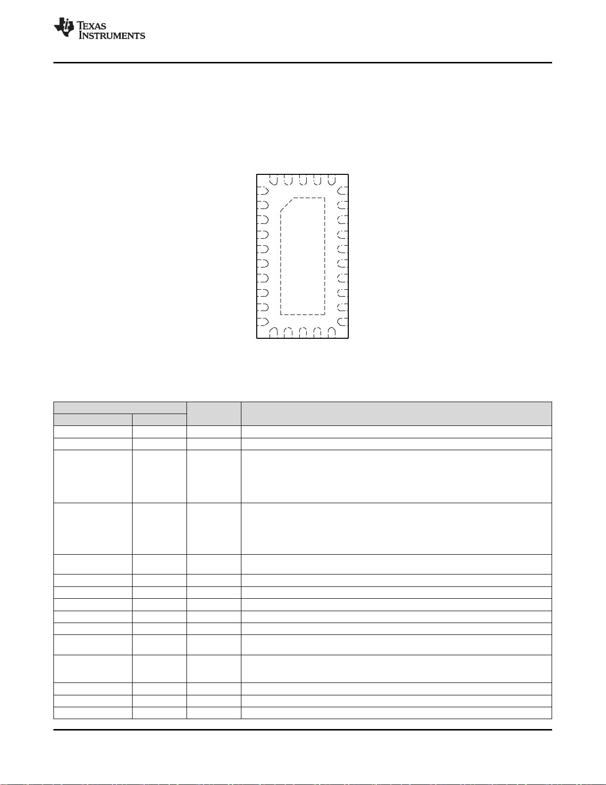
5 Pin Configuration and Functions......................... 3
6 Specifications......................................................... 5
6.1 Absolute Maximum Ratings ...................................... 5
6.2 ESD Ratings.............................................................. 5
6.3 Recommended Operating Conditions....................... 5
6.4 Thermal Information.................................................. 6
6.5 Electrical Characteristics........................................... 6
6.6 Timing Requirements................................................ 8
7 Detailed Description............................................ 10
7.1 Overview ................................................................. 10
7.2 Functional Block Diagram ....................................... 12
7.3 Feature Description................................................. 13
7.4 Device Functional Modes........................................ 16
7.5 Programming........................................................... 18
7.6 Register Maps ........................................................ 19
8 Application and Implementation ........................ 23
8.1 Application Information............................................ 23
8.2 Typical Application, DRP Port ................................ 24
9 Power Supply Recommendations...................... 29
10 Layout................................................................... 30
10.1 Layout Guidelines ................................................. 30
10.2 Layout ................................................................... 36
11 器器件件和和文文档档支支持持 ..................................................... 37
11.1 接收文档更新通知 ................................................. 37
11.2 社区资源................................................................ 37
11.3 商标 ....................................................................... 37
11.4 静电放电警告......................................................... 37
11.5 Glossary................................................................ 37
12 机机械械、、封封装装和和可可订订购购信信息息....................................... 37
4 修修订订历历史史记记录录
Changes from Original (December 2016) to Revision A Page
• Absolute Maximum Ratings, Deleted "ENn_MUX" from the Control Pins.............................................................................. 5
• ESD Ratings, Deleted text "Pins listed as ± XXX V may actually have higher performance." from Note 1............................ 5
• Recommended Operating Conditions, Added "VDD5 supply ramp time" ............................................................................. 5
• Recommended Operating Conditions, Changed "External resistor on VBUS_DET pin" MIN value From: 890 KΩ To:
880 KΩ.................................................................................................................................................................................... 5
• Switch the position of CC1 and CC2 in Figure 10 ............................................................................................................... 24
• Switch the position of CC1 and CC2 in Figure 11 ............................................................................................................... 26
• Switch the position of CC1 and CC2 in Figure 12 ............................................................................................................... 28

CC1
CC2
CURRENT_MODE
PORT
VBUS_DET
RXp
RXn
TXp
TXn
VCC33
RX1p
RX1n
TX1p
TX1n
RX2p
RX2n
TX2p
TX2n
GND GND
ENn_CC
VDD5
ID
SCL/OUT2
SDA/OUT1
VCONN_FAULT_N
INT_N/OUT3
ADDR
ENn_MUX
DIR
30
11
29
12
28
13
27
14
1
2
3
4
5
6
7
8
9
10 16
17
18
19
20
21
22
23
24
25
26
15
Thermal
Pad
3
HD3SS3220
www.ti.com.cn
ZHCSFC4A –DECEMBER 2015–REVISED AUGUST 2016
Copyright © 2015–2016, Texas Instruments Incorporated
5 Pin Configuration and Functions
RNH Package
30 Pin (VQFN)
Top View
Pin Functions
PIN
I/O DESCRIPTION
NAME NO.
CC2 1 I/O Type-C Configuration channel signal 2
CC1 2 I/O Type-C Configuration channel signal 1
CURRENT_MODE 3 I
Tri-level input pin to indicate current advertisement in DFP (or DFP in DRP) mode while in GPIO
mode. Don’t care in UFP mode. Provides the flexibility to advertise higher current without I
2
C. The
pin has 250 K internal pull-down.
L – Low - Default – 900 mA
M - Medium (Install 500 K to VDD on the PCB) – 1.5 A
H - High (Install 10 K to VDD on the PCB) – 3 A
PORT 4 I
Tri-level input pin to indicate port mode. The state of this pin is sampled when HD3SS3220’s
ENn_CC is asserted low, and VDD is active. This pin is also sampled following a
I2C_SOFT_RESET.
H - DFP (Pull-up to VDD if DFP mode is desired)
NC - DRP (Leave unconnected if DRP mode is desired)
L - UFP (Pull-down or tie to GND if UFP mode is desired)
VBUS_DET 5 I
5-28V VBUS input voltage. VBUS detection determines UFP attachment. One 900K external
resistor required between system VBUS and VBUS_DET pin.
TXp 6 I/O Host/Device USB SuperSpeed differential Signal TX positive
TXn 7 I/O Host/Device USB SuperSpeed differential Signal TX negative
VCC33 8 P 3.3-V Power supply
RXp 9 I/O Host/Device USB SuperSpeed differential Signal RX positive
RXn 10 I/O Host/Device USB SuperSpeed differential Signal RX negative
DIR 11 O
Type-C plug orientation. Open drain output.
A pull-up resistor (that is, 200 K) must be installed for proper operation of the device.
ENn_MUX 12 I
Active Low MUX Enable:
L - Normal operation, and
H - Shutdown.
GND 13, 28 G Ground
RX1n 14 I/O Type-C Port - USB SuperSpeed differential Signal RX1 negative
RX1p 15 I/O Type-C Port - USB SuperSpeed differential Signal RX1 positive

4
HD3SS3220
ZHCSFC4A –DECEMBER 2015–REVISED AUGUST 2016
www.ti.com.cn
Copyright © 2015–2016, Texas Instruments Incorporated
Pin Functions (continued)
PIN
I/O DESCRIPTION
NAME NO.
TX1n 16 I/O Type-C Port - USB SuperSpeed differential Signal TX1 negative
TX1p 17 I/O Type-C Port - USB SuperSpeed differential Signal TX1 positive
RX2n 18 I/O Type-C Port - USB SuperSpeed differential Signal RX2 negative
RX2p 19 I/O Type-C Port - USB SuperSpeed differential Signal RX2 positive
TX2n 20 I/O Type-C Port - USB SuperSpeed differential Signal TX2 negative
TX2p 21 I/O Type-C Port - USB SuperSpeed differential Signal TX2 positive
ADDR 22 I
Tri-level input pin to indicate I
2
C address or GPIO mode:
H (connect to VDD5) - I
2
C is enabled and I2C 7-bit address is 0x67.
NC - GPIO mode (I2C is disabled)
L (connect to GND) - I
2
C is enabled and I2C 7-bit address is 0x47.
ADDR pin should be pulled up to VDD if high configuration is desired
INT_N/OUT3 23 O
The INT_N/OUT3 is a dual-function pin.
When used as the INT_N, the pin is an open drain output in I
2
C control mode and is an active low
interrupt signal for indicating changes in I
2
C registers.
When used as OUT3, the pin is in audio accessory detect in GPIO mode:
H - no detection, and
L - audio accessory connection detected.
VCONN_FAULT_N 24 O Open drain output. Asserted low when VCONN overcurrent detected.
SDA/OUT1 25 I/O
The SDA/OUT1 is a dual-function pin.
When I2C is enabled (ADDR pin is high or low), this pin is the I
2
C communication data signal.
When in GPIO mode (ADDR pin is NC), this pin is an open drain output for communicating Type-C
current mode detect when the device is in UFP mode:
H – Default (900 mA) current mode detected, and
L – Medium (1.5 A) or High (3 A) Current Mode detected.
SCL/OUT2 26 I/O
The SCL/OUT2 is a dual function pin.
When I
2
C is enabled (ADDR pin is high or low), this pin is the I
2
C communication clock signal.
When in GPIO mode (ADDR pin is NC), this pin is an open drain output for communicating Type-C
current mode detect when the device is in UFP mode:
H – Default or Medium current mode detected, and
L – High current mode detected.
ID 27 O
Open drain output. Asserted low when CC pin detected device attachment when port is a source
(DFP), or dual-role (DRP) acting as source (DFP).
ENn_CC 29 I Enable signal for CC controller. Enable is active low.
VDD5 30 P 5-V Power supply
Thermal Pad – –
The thermal PAD must be connected to GND, see the Thermal Pad connection techniques
(SLMA002).

5
HD3SS3220
www.ti.com.cn
ZHCSFC4A –DECEMBER 2015–REVISED AUGUST 2016
Copyright © 2015–2016, Texas Instruments Incorporated
(1) Stresses beyond those listed under Absolute Maximum Ratings may cause permanent damage to the device. These are stress ratings
only, which do not imply functional operation of the device at these or any other conditions beyond those indicated under Recommended
Operating Conditions. Exposure to absolute-maximum-rated conditions for extended periods may affect device reliability.
6 Specifications
6.1 Absolute Maximum Ratings
over operating free-air temperature range (unless otherwise noted)
(1)
MIN MAX UNIT
5-V Supply Voltage VDD5 –0.3 6 V
3.3-V Supply Voltage VCC33 –0.3 4 V
Control Pins
CC1, CC2, ADDR, PORT, ID, DIR,
INT_N/OUT3, ENn_CC, SDA/OUT1,
SCL/OUT2
–0.3 VDD5 +0.3 V
ENn_MUX, DIR –0.3 VCC33 +0.3 V
VBUS_DET –0.3 4 V
Super-speed Differential Signal Pins [RX/TX] [p/n], [RX/TX][2/1][p/n] –0.3 2.5 V
Storage temperature, T
stg
–65 150 °C
(1) JEDEC document JEP155 states that 500-V HBM allows safe manufacturing with a standard ESD control process. Manufacturing with
less than 500-V HBM is possible with the necessary precautions.
(2) JEDEC document JEP157 states that 250-V CDM allows safe manufacturing with a standard ESD control process..
6.2 ESD Ratings
VALUE UNIT
V
(ESD)
Electrostatic discharge
Human-body model (HBM), per ANSI/ESDA/JEDEC JS-001
(1)
±2000
V
Charged-device model (CDM), per JEDEC specification JESD22-
C101
(2)
±1500
(1) With 200 mA VCONN current for VCONN ≥ 4.75 V at connector, VDD5 ≥ 5 V is recommended
6.3 Recommended Operating Conditions
over operating free-air temperature range (unless otherwise noted)
MIN NOM MAX UNIT
V
DD5
5-V Supply Voltage range 4.5
(1)
5.5 V
V
CC33
3.3-V Supply Voltage range 3 3.6 V
V
DD
Supply range for I2C (SDA, SCL) pins 1.65 3.6 V
V
DD5(ramp)
VDD5 supply ramp time 25 ms
V
(diff)
High speed signal pins differential voltage 0 1.8 V
PP
V
(cm)
High speed signal pins common mode voltage 0 2 V
T
A
Operating free-air/ambient temperature (HD3SS3220) 0 70 °C
T
A
Operating free-air/ambient temperature (HD3SS3220I) –40 85 °C
V
(BUS)
System V
(BUS)
input voltage through 900-K resistor 4 5 28 V
C
(BULK)
Bulk capacitance on VCONN. Only when VCONN is on.
Disconnected when VCONN is off. Shall be placed on VDD5.
10 200 µF
R
(p_ODext)
External Pull up resistor on Open Drain IOs (OUT1, OUT2,
INT/OUT3, ID, VCONN_FAULT_N, and DIR pins)
200 KΩ
R
(p_TLext)
Tri-level input external pull-up resistor (PORT and ADDR pins) 4.7 KΩ
R
(p_15A)
External pull up resistor to advertise 1.5 A (CURRENT_MODE pin) 500 KΩ
R
(p_3A)
External pull up resistor to advertise 3 A (CURRENT_MODE pin) 10 KΩ
R
(p_i2c_ext)
External Pull up resistance on I
2
C bus
(Could be 4.7 K or higher. Nominal value listed)
2.2 KΩ
R
(VBUS)
External resistor on VBUS_DET pin 880 900 910 KΩ
C
(bus,I2c)
Total capacitive load for each I
2
C bus line 400 pF
剩余42页未读,继续阅读
资源评论

不觉明了
- 粉丝: 691
- 资源: 4046

上传资源 快速赚钱
我的内容管理 收起
我的资源 快来上传第一个资源
我的收益
登录查看自己的收益我的积分 登录查看自己的积分
我的C币 登录后查看C币余额
我的收藏
我的下载
下载帮助

会员权益专享
安全验证
文档复制为VIP权益,开通VIP直接复制
