TI-BQ2026.pdf
需积分: 10 61 浏览量
2022-10-31
21:52:00
上传
评论 5
收藏 1.4MB PDF 举报

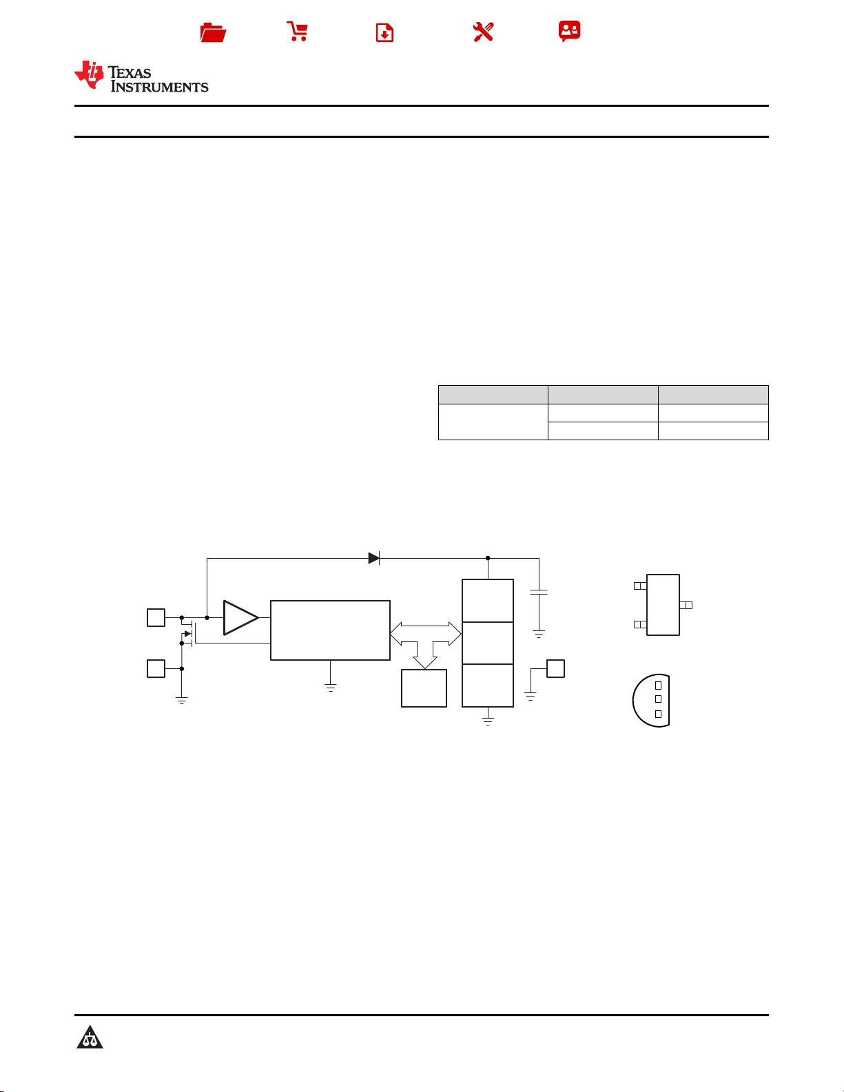
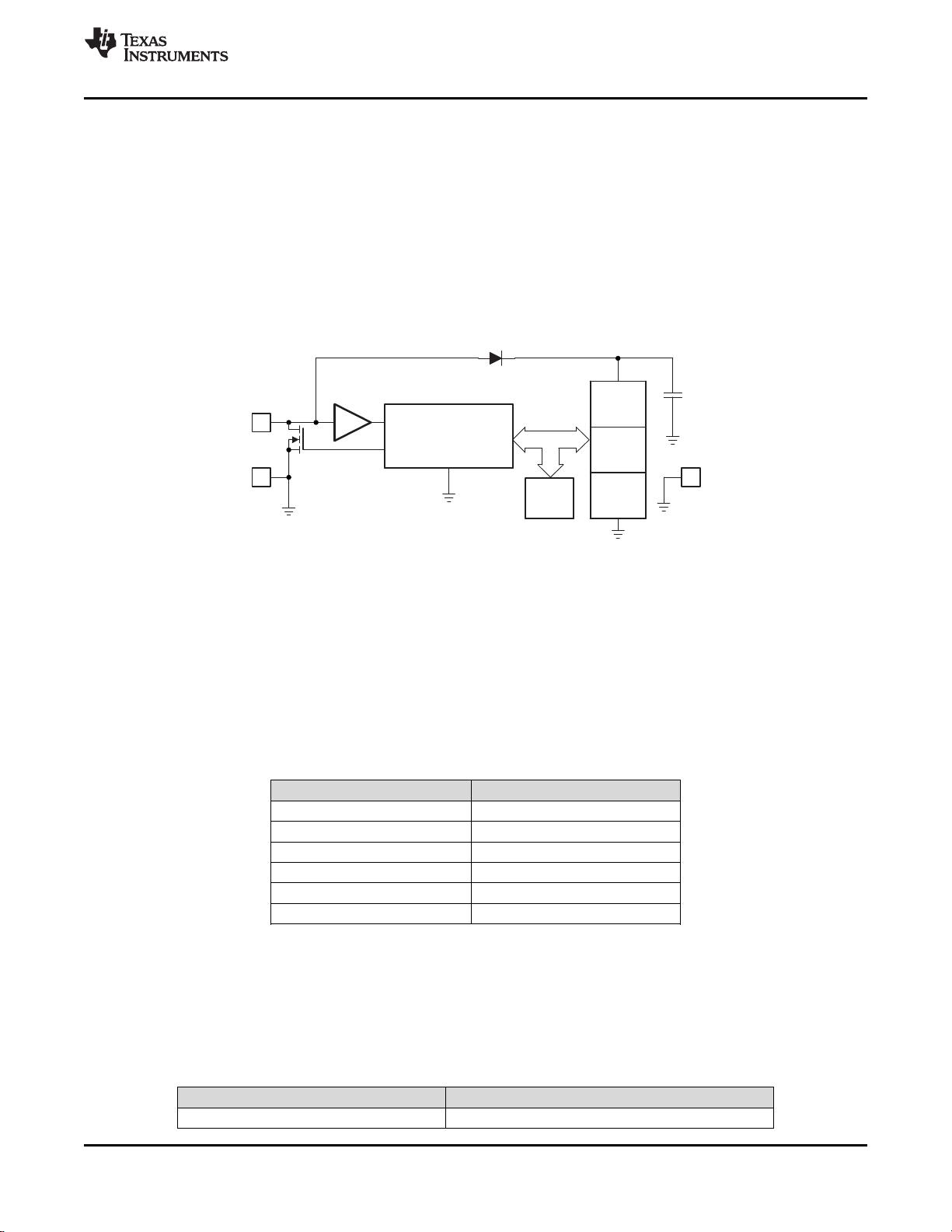
DBZ Package
(Top View)
LP Package
(BottomView)
ID ROM
(64 bits)
EPROM
Memory
(1536 bits)
EPROM
Status
(64 bits)
SDQ Communications
Controller and CRC
Generation Circuit
Internal
Bus
RAM
Buffer
(1 byte)
SDQ
VSS VSS
VSS
SDQ
VSS
1
2
3
1
VSS
2
3
VSS
SDQ
Product
Folder
Sample &
Buy
Technical
Documents
Tools &
Software
Support &
Community
bq2026
ZHCS608A –DECEMBER 2011–REVISED OCTOBER 2014
具具有有 SDQ 接接口口的的 1.5K 位位串串行行 EPROM
1 特特性性 3 说说明明
1
• 1536 位的一次性可编程 (OTP) EPROM,用于存
bq2026 是一款 1.5K 位串行 EPROM,此器件包含一
储用户可编程的配置数据
个厂家设定,唯一 48 位识别号,8 位产品编码,和一
• 厂家设定的唯一 64 位识别号
个 64 位状态寄存器。
• 单线制接口以减少电路板布线
bq2026 SDQ™ 接口只要求一个单一连接和一个接地
• 同步通信减少主机中断开销
返回。 SDQ 引脚也是 bq2026 的唯一电源。
• 在数据引脚上的 6KV IEC 61000-4-2 静电放电
(ESD)兼容性
该器件提供小型表面贴装选项,可节省在印刷电路板上
• 无需待机电源
的占用空间,同时拥有低成本优势,非常适合电池组配
• 采用 3 引脚 SOT-23 和 TO-92 封装
置参数、记录保存、资产跟踪、产品版本状态以及代码
访问安全性等应用。
2 应应用用
器器件件信信息息
(1)
• 安全编码
器器件件型型号号 封封装装 封封装装尺尺寸寸((标标称称值值))
• 库存跟踪
SOT-23 (3) 4.30mm × 4.30mm
• 产品修正维护
bq2026
TO-92 (3) 2.92mm × 1.30mm
• 电池组识别
(1) 要了解所有可用封装,请见数据表末尾的封装选项附录。
框框图图
注:可将 LP 封装的引脚 3 接地或保持悬空。
1
An IMPORTANT NOTICE at the end of this data sheet addresses availability, warranty, changes, use in safety-critical applications,
intellectual property matters and other important disclaimers. PRODUCTION DATA.
English Data Sheet: SLUS938

剩余27页未读,继续阅读
资源评论


