TI-BQ4017.pdf
需积分: 9 66 浏览量
2022-12-10
23:23:04
上传
评论 4
收藏 553KB PDF 举报

Features
➤
Data retention in the absence of
power
➤
Automatic write-protection dur
-
ing power-up/power-down cycles
➤
Conventional SRAM operation;
unlimited write cycles
➤
5-year minimum data retention
in absence of power
➤
Battery internally isolated until
power is applied
General Description
The CMOS bq4017 is a nonvolatile
16,777,216-bit static RAM organized
as 2,097,152 words by 8 bits. The
integral control circuitry and lith
-
ium energy source provide reliable
nonvolatility coupled with the un
-
limited write cycles of standard
SRAM.
The control circuitry constantly
monitors the single 5V supply for an
out-of-tolerance condition. When V
CC
falls out of tolerance, the SRAM is
unconditionally write-protected to
prevent an inadvertent write opera
-
tion.
At this time the integral energy
source is switched on to sustain the
memory until after V
CC
returns valid.
The bq4017 uses extremely low
standby current CMOS SRAMs, cou
-
pled with small lithium coin cells to
provide nonvolatility without long
write-cycle times and the write-cycle
limitations associated with EE
-
PROM.
The bq4017 has the same interface
as industry-standard SRAMs and
requires no external circuitry.
1
Selection Guide
Part
Number
Maximum
Access
Time (ns)
Negative
Supply
Tolerance
Part
Number
Maximum
Access
Time (ns)
Negative
Supply
Tolerance
bq4017MC -70 70 -5% bq4017YMC -70 70 -10%
1
PN401701.eps
36-Pin DIP Module
2
3
4
5
6
7
8
9
10
11
12
13
14
15
16
17
18
36
35
34
33
32
31
30
29
28
27
26
25
24
23
22
21
20
19
NC
A
20
A
18
A
16
A
14
A
12
A
7
A
6
A
5
A
4
A
3
A
2
A
1
A
0
DQ
1
DQ
2
V
SS
DQ
0
V
CC
A
19
NC
A
15
A
17
WE
A
13
A
8
A
9
A
11
OE
A
10
CE
DQ
7
DQ
5
DQ
4
DQ
3
DQ
6
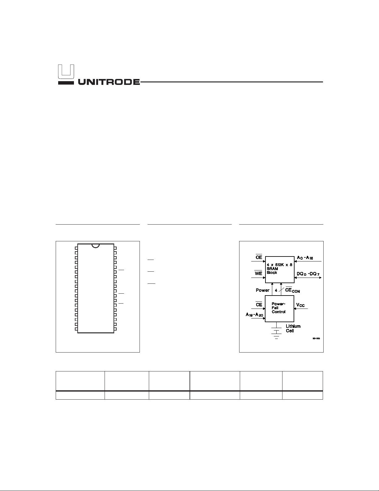
Pin Names
A
0
–A
20
Address inputs
DQ
0
–DQ
7
Data input/output
CE
Chip enable input
OE
Output enable input
WE
Write enable input
V
CC
Supply voltage input
V
SS
Ground
NC No connect
Block Diagram
bq4017/bq4017Y
5/95
Pin Connections
2048Kx8 Nonvolatile SRAM
剩余11页未读,继续阅读
资源评论


