TI-BQ4015.pdf
需积分: 0 72 浏览量
2022-12-10
23:24:59
上传
评论 4
收藏 518KB PDF 举报


1
Features
➤
Data retention for at least 10
years without power
➤
Automatic write-protection during
power-up/power-down cycles
➤
Conventional SRAM operation,
including unlimited write cycles
➤
Internal isolation of battery be
-
fore power application
➤
Industry standard 32-pin DIP
pinout
➤
34-pin LIFETIME LITHIUM™
module
-
Module completely
surface-mounted
-
Snap-on power-source for
lithium battery backup
-
Replaceable power-source
(part number: bq40MS)
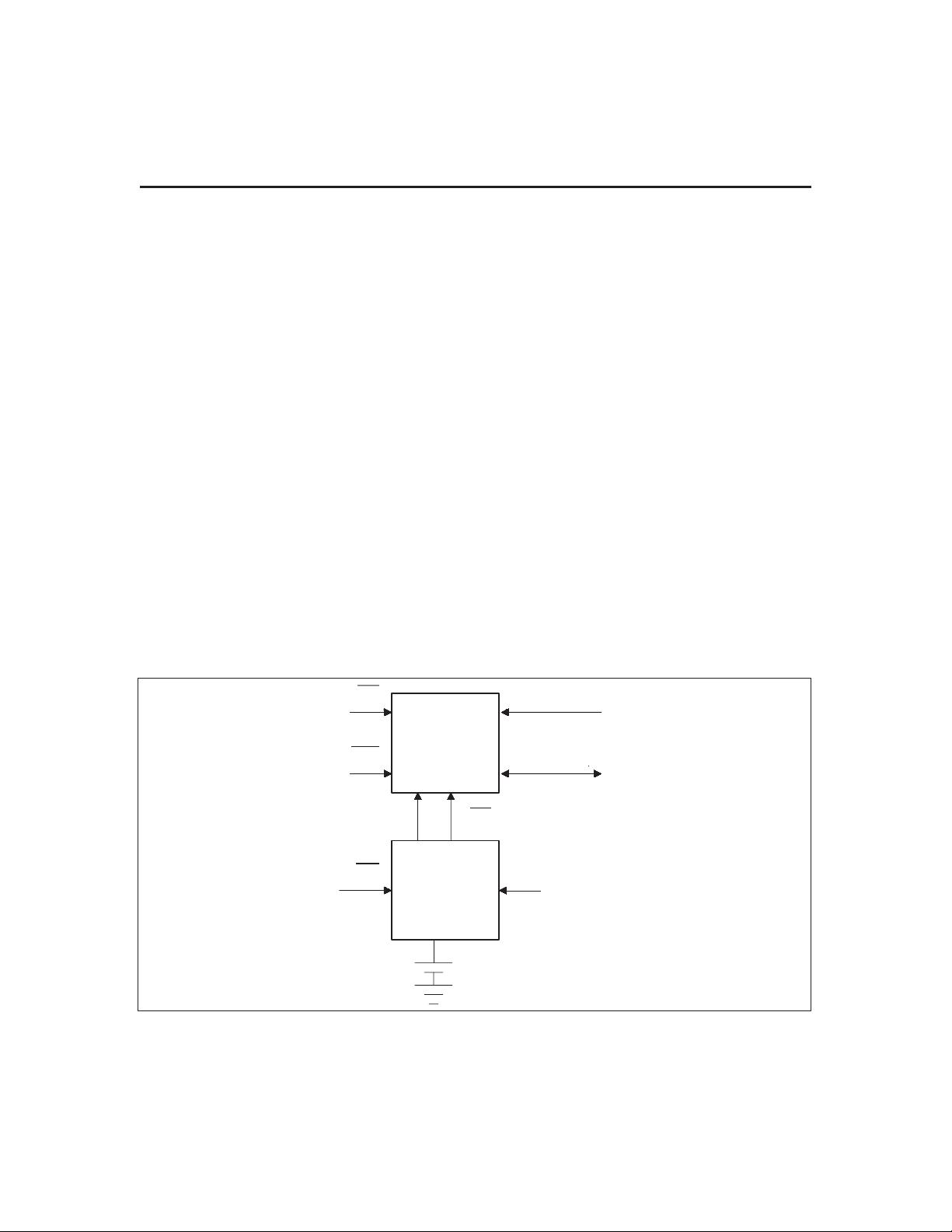
General Description
The CMOS bq4015/Y is a nonvola
-
tile 4,194,304-bit static RAM organ
-
ized as 524,288 words by 8 bits. The
integral control circuitry and lith
-
ium energy source provide reliable
nonvolatility coupled with the un
-
limited write cycles of standard
SRAM.
The control circuitry constantly
monitors the single 5V supply for an
out-of-tolerance condition. When
V
CC
falls out of tolerance, the SRAM
is unconditionally write-protected to
prevent an inadvertent write opera
-
tion.
At this time the integral energy
source is switched on to sustain the
memory until after V
CC
returns
valid.
The bq4015/Y uses extremely low
standby current CMOS SRAMs, cou
-
pled with small lithium coin cells to
provide nonvolatility without long
write-cycle times and the write-cycle
limitations associated with EE
-
PROM.
The bq4015/Y requires no external
circuitry and is compatible with the
industry-standard 4Mb SRAM pin
-
out.
1
PN401501.eps
32-Pin DIP Module
2
3
4
5
6
7
8
32
31
30
29
28
27
26
25
9
10
24
23
11
12
22
21
13
14
20
19
15
16
18
17
V
CC
A
15
A
17
WE
A
13
A
8
A
9
A
11
OE
A
10
CE
DQ
7
DQ
6
DQ
5
DQ
4
DQ
3
A
18
A
16
A
14
A
12
A
7
A
6
A
5
A
4
A
3
A
2
A
1
A
0
DQ
0
DQ
1
DQ
2
V
SS
Pin Names
A0–A18 Address inputs
DQ0–DQ7 Data input/output
CE
Chip enable input
OE
Output enable input
WE
Write enable input
NC No connect
V
CC
Supply voltage input
V
SS
Ground
bq4015/Y
5/99 E
Pin Connections
512Kx8 Nonvolatile SRAM
PN4015Yncm.eps
34-Pin LIFETIME LITHIUM Module
11
12
13
14
15
16
17
1
2
3
4
5
6
7
8
9
10
24
23
22
21
20
19
18
34
33
32
31
30
29
28
27
26
25
NC
A15
A16
NC
V
CC
WE
OE
CE
DQ
7
DQ
6
DQ
5
DQ
4
DQ
3
DQ
2
DQ
1
DQ
0
V
SS
A18
A17
A14
A13
A12
A11
A10
A9
A8
A7
A6
A5
A4
A3
A2
A1
A0
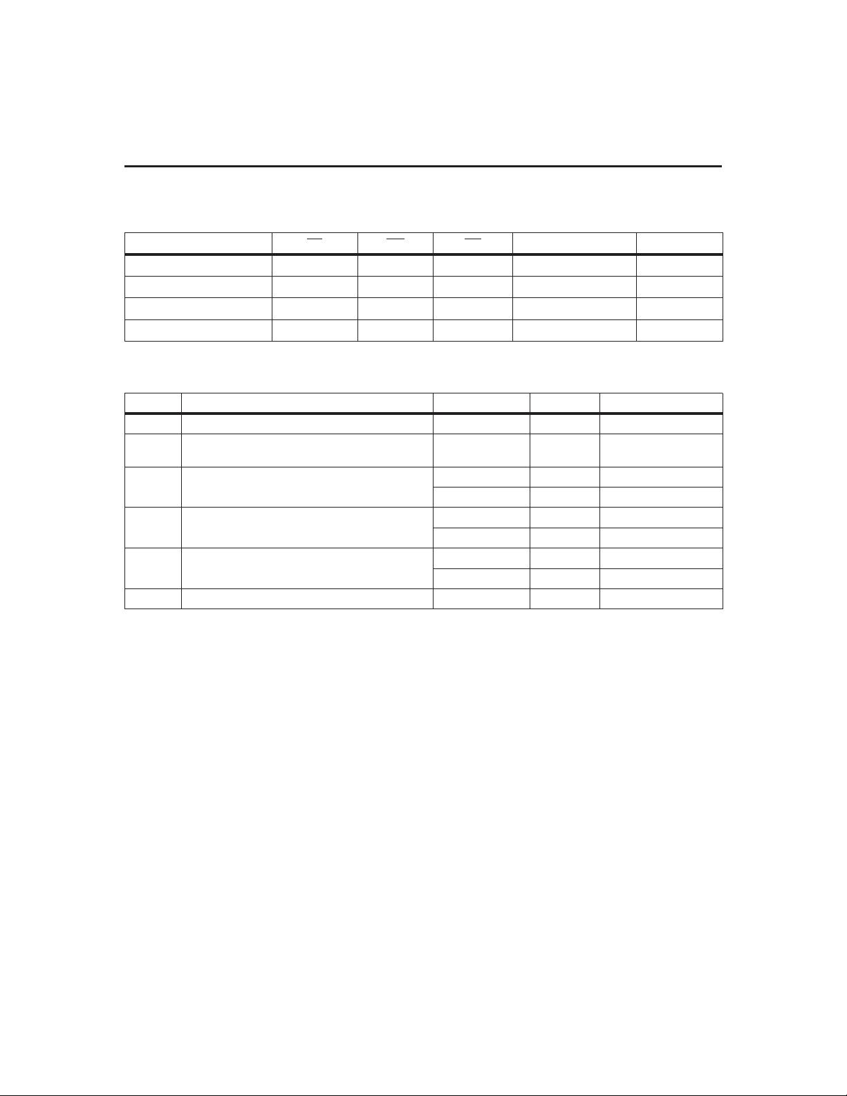
Selection Guide
Part
Number
Maximum
Access
Time (ns)
Negative
Supply
Tolerance
Part
Number
Maximum
Access
Time (ns)
Negative
Supply
Tolerance
bq4015x -70 70 -5% bq4015Yx -70 70 -10%
bq4015x -85 85 -5% bq4015Yx -85 85 -10%
Note: x = MA for PDIP or MS for LIFETIME LITHIUM module.
剩余12页未读,继续阅读
资源评论


