TI-BQ500101.pdf

V
SW
Current (A)
Efficiency (%)
Power Loss (W)
0 2 4 6 8 10
60 0
65 0.4
70 0.8
75 1.2
80 1.6
85 2
90 2.4
95 2.8
100 3.2
D001
V
DD
= 5 V
V
IN
= 10 V
L
SW
= 6 PH
f
SW
= 130 kHz
T
A
= 25qC
Duty Cycle = 50%
Efficiency (%)
Power Loss (W)
bq500101
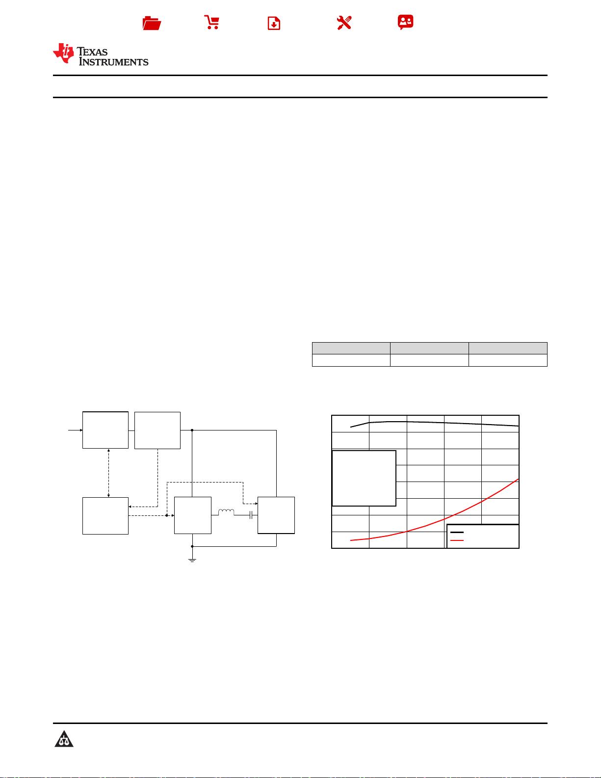
(Voltage Regulation)
19 V
bq500100
(Current Sense
Monitor)
bq500101
bq500101
bq501210
(Wireless Power
Transmitter Controller)
Product
Folder
Sample &
Buy
Technical
Documents
Tools &
Software
Support &
Community
An IMPORTANT NOTICE at the end of this data sheet addresses availability, warranty, changes, use in safety-critical applications,
intellectual property matters and other important disclaimers. PRODUCTION DATA.
English Data Sheet: SLPS585
bq500101
ZHCSEQ6 –MARCH 2016
bq500101 NexFET™功功率率级级
1
1 特特性性
1
• 5A 电流时系统效率达 98%
• 最大额定持续电流 10A,峰值 15A
• 高频工作(高达 600kHz)
• 高密度小外形尺寸无引线 (SON) 3.5mm x 4.5mm
封装
• 超低电感封装
• 系统已优化的印刷电路板 (PCB) 封装
• 3.3V 和 5V 脉宽调制 (PWM) 信号兼容
• 输入电压高达 24V
• 集成型自举二极管
• 击穿保护
• 符合 RoHS 绿色环保标准-无铅引脚镀层
• 无卤素
• 包含高效栅极驱动器和场效应管 (FET) 的优化型功
率级
• 针对 15W 无线电源发射器设计进行了优化
2 应应用用
• 用于 15W 或 5W 系统的无线电源发射器,符合
WPC (Qi) 1.2 规范
• 专用无线充电器和发射器
• 以无线方式供电的工业和医疗系统
• 更多相关信息,请访问 www.ti.com/wirelesspower
3 说说明明
bq500101 NexFET™功率级针对涵盖 WPC v1.2 中等
功率规范的无线电源 应用 进行了优化。该器件既可用
于固定频率发射器类型中的电源轨电压控制,也可用于
固定频率和频率可变两种发射器类型中的线圈驱动器。
这个组合在小型 3.5mm x 4.5mm 外形尺寸封装中实现
具有高电流、高效率和高速开关功能的器件。此外,印
刷电路板 (PCB) 封装已经过优化,可帮助减少设计时
间并简化总体系统设计的完成。
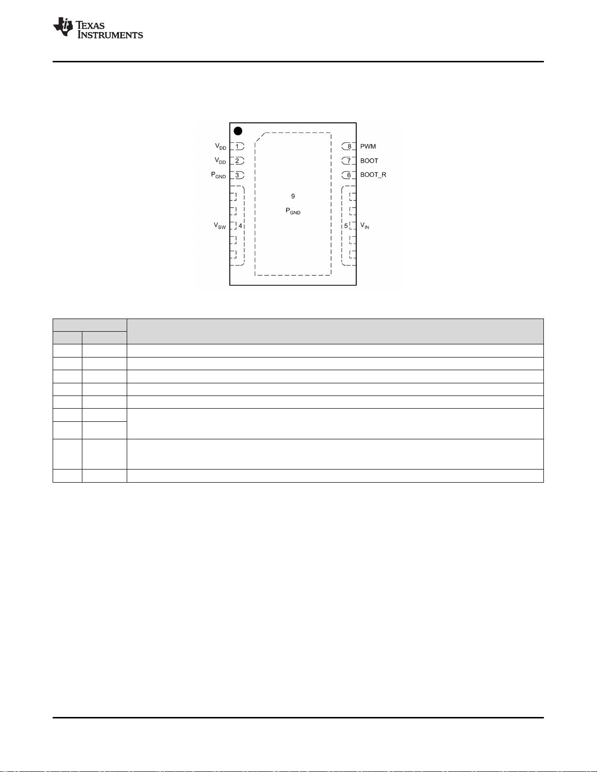
器器件件信信息息
(1)
订订货货编编号号 封封装装 封封装装尺尺寸寸((标标称称值值))
bq500101 DPC (9) 3.5mm x 4.5mm
(1) 要了解所有可用封装,请见数据表末尾的可订购产品附录。
空白
应应用用图图表表 典典型型功功率率级级效效率率与与功功率率损损耗耗

剩余20页未读,继续阅读


评论1
最新资源