TI-BQ25123.pdf
需积分: 9 68 浏览量
2022-11-20
17:12:14
上传
评论 5
收藏 3.2MB PDF 举报

BQ25123 700-nA Low Iq Highly Integrated Battery Charge Management Solution for
Wearables
1 Features
• Increases system operation time between charges
– Configurable 300-mA buck regulator
– 700-nA (typical) Iq with buck converter enabled
(no load)
– Configurable load switch or 100-mA LDO
output
– Up to 300-mA charge current for fast charging
– 0.5% accurate battery voltage regulation
(configurable from 3.6 V to 4.65 V in 10-mV
steps)
– Configurable termination current down to
500 µA
– Simple voltage based battery monitor
• Highly integrated solution with small footprint
– 2.5 mm x 2.5 mm WCSP package and 6
external components for minimal solution
– Push-button wake-up and reset with adjustable
timers
– Power path management for powering the
system and charging the battery
– Power path management enables <50-nA Ship
Mode battery quiescent current for longest shelf
life
– Battery charger operates from 3.4 V – 5.5 V
IN
(5.5-V OVP / 20-V tolerant)
– Dedicated pins for input current limit, charge
current, termination current, and status output
• I
2
C communication control
– Charge voltage and current
– Termination threshold
– Input current limit
– VINDPM threshold
– Timer options
– Load switch control
– Controls for interrupts for faults and status
– System output voltage adjustment
– LDO output voltage adjustment
2 Applications
• Smart watches and other wearable devices
• Fitness accessories
• Health monitoring medical accessories
• Rechargeable toys
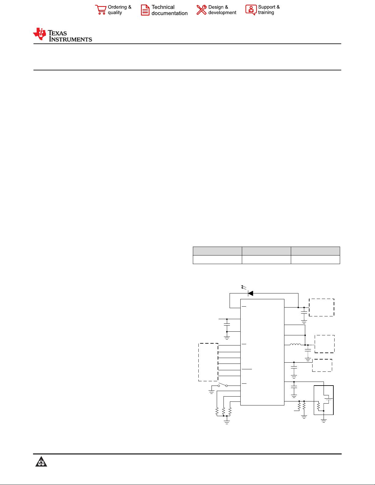
3 Description
The BQ25123 is a highly integrated battery charge
management IC that integrates the most common
functions for wearable devices: Linear charger,
regulated output, load switch, manual reset with timer,
and battery voltage monitor. The integrated buck
converter is a high efficiency, low I
Q
switcher using
DCS control that extends light load efficiency down to
10-µA load currents. The low quiescent current during
operation and shutdown enables maximum battery
life. The device supports charge currents from 5 mA
to 300 mA. The input current limit, charge current,
buck converter output voltage, LDO output voltage,
and other parameters are programmable through the
I
2
C interface.
Device Information
(1)
PART NUMBER PACKAGE BODY SIZE (NOM)
BQ25123 DSBGA (25) 2.50 mm x 2.50 mm
(1) For all available packages, see the orderable addendum at
the end of the data sheet.
BQ25123
GND
HOST
SDA
SCL
INT
SW
BAT
MCU /
SYSTEM
-+
NTC
TS
LS / LDO
<100mA
Load
IN
SYS
LSCTRL
VINLS
Unregulated
Load
PMID
IPRETERM
ISET
ILIM
IN
PG
CD
RESET
MR
Simplified Schematic
BQ25123
SLUSCZ6A – JANUARY 2018 – REVISED MAY 2021
An IMPORTANT NOTICE at the end of this data sheet addresses availability, warranty, changes, use in safety-critical applications,
intellectual property matters and other important disclaimers. PRODUCTION DATA.


剩余71页未读,继续阅读


评论0
最新资源