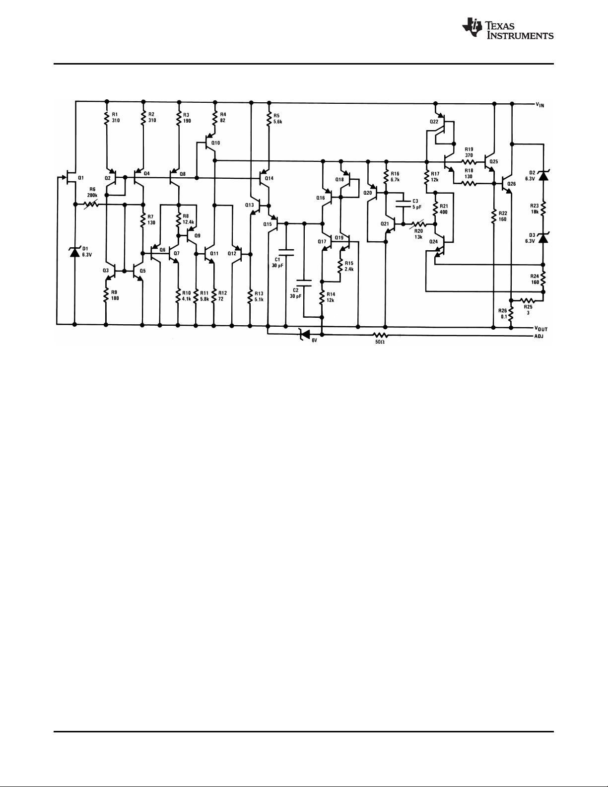
没有合适的资源?快使用搜索试试~ 我知道了~
TI-LM117JAN.pdf
需积分: 9 0 下载量 136 浏览量
2022-10-28
21:19:43
上传
评论 5
收藏 966KB PDF 举报
温馨提示
试读
24页
TI-LM117JAN.pdf
资源推荐
资源详情
资源评论
LM117JAN
www.ti.com
SNVS365A –MARCH 2006–REVISED MARCH 2013
LM117JAN 3-Terminal Adjustable Regulator
Check for Samples: LM117JAN
Also, it makes an especially simple adjustable
1
FEATURES
switching regulator, a programmable output regulator,
2
• Specified 0.5A or 1.5A Output Current
or by connecting a fixed resistor between the
• Adjustable Output Down to 1.2V
adjustment pin and output, the LM117 can be used
as a precision current regulator. Supplies with
• Current Limit Constant with Temperature
electronic shutdown can be achieved by clamping the
• 80 dB Ripple Rejection
adjustment terminal to ground which programs the
• Output is Short-circuit Protected
output to 1.2V where most loads draw little current.
For the negative complement, see LM137 series data
DESCRIPTION
sheet.
The LM117 adjustable 3-terminal positive voltage
regulator is capable of supplying either 0.5A or 1.5A
Connection Diagrams
over a 1.2V to 37V output range. It is exceptionally
easy to use and requires only two external resistors
to set the output voltage. Further, both line and load
regulation are better than standard fixed regulators.
In addition to higher performance than fixed
regulators, the LM117 series offers full overload
protection available only in IC's. Included on the chip
are current limit, thermal overload protection and safe
area protection. All overload protection circuitry
CASE IS OUTPUT
remains fully functional even if the adjustment
Figure 1. (TO-3)
terminal is disconnected.
Metal Can Package
Normally, no capacitors are needed unless the device
Bottom View
is situated more than 6 inches from the input filter
Steel Package
capacitors in which case an input bypass is needed. Package Number K0002C
An optional output capacitor can be added to improve
transient response. The adjustment terminal can be
bypassed to achieve very high ripple rejection ratios
which are difficult to achieve with standard 3-terminal
regulators.
Besides replacing fixed regulators, the LM117 is
useful in a wide variety of other applications. Since
CASE IS OUTPUT
the regulator is “floating” and sees only the input-to-
output differential voltage, supplies of several
Figure 2. (TO)
hundred volts can be regulated as long as the
Metal Can Package
maximum input to output differential is not exceeded,
Bottom View
i.e., avoid short-circuiting the output.
Package Number NDT0003A
Table 1. LM117 Series Packages
Part Number Suffix Package Design Load Current
K TO-3 1.5A
NDT TO 0.5A
1
Please be aware that an important notice concerning availability, standard warranty, and use in critical applications of
Texas Instruments semiconductor products and disclaimers thereto appears at the end of this data sheet.
2All trademarks are the property of their respective owners.
PRODUCTION DATA information is current as of publication date.
Copyright © 2006–2013, Texas Instruments Incorporated
Products conform to specifications per the terms of the Texas
Instruments standard warranty. Production processing does not
necessarily include testing of all parameters.
LM117JAN
www.ti.com
SNVS365A –MARCH 2006–REVISED MARCH 2013
These devices have limited built-in ESD protection. The leads should be shorted together or the device placed in conductive foam
during storage or handling to prevent electrostatic damage to the MOS gates.
Absolute Maximum Ratings
(1)
Power Dissipation
(2)
Internally Limited
Input-Output Voltage Differential +40V, −0.3V
Storage Temperature −65°C ≤ T
A
≤ +150°C
Maximum Junction Temperature (T
Jmax
) +150°C
Lead Temperature Metal Package 300°C
Thermal Resistance
θ
JA
TO–3 Still Air 39°C/W
TO–3 500LF/Min Air flow 14°C/W
TO Still Air 186°C/W
TO 500LF/Min Air flow 64°C/W
θ
JC
TO–3 1.9°C/W
TO Metal Can 21°C/W
ESD Tolerance
(3)
3KV
(1) Absolute Maximum Ratings indicate limits beyond which damage to the device may occur. Operating Ratings indicate conditions for
which the device is functional, but do not ensure specific performance limits. For ensured specifications and test conditions, see the
Electrical Characteristics. The ensured specifications apply only for the test conditions listed. Some performance characteristics may
degrade when the device is not operated under the listed test conditions.
(2) The maximum power dissipation must be derated at elevated temperatures and is dictated by T
Jmax
(maximum junction temperature),
θ
JA
(package junction to ambient thermal resistance), and T
A
(ambient temperature). The maximum allowable power dissipation at any
temperature is P
Dmax
= (T
Jmax
- T
A
)/θ
JA
or the number given in the Absolute Maximum Ratings, whichever is lower. "Although power
dissipation is internally limited, these specifications are applicable for power dissipations of 2W for the TO package and 20W for the TO-
3 package."
(3) Human body model, 100 pF discharged through a 1.5 kΩ resistor.
Recommended Operating Conditions
Operating Temperature Range −55°C ≤ T
A
≤ +125°C
Input Voltage Range 4.25V to 41.25V
Quality Conformance Inspection
MIL-STD-883, Method 5005 - Group A
Subgroup Description Temp °C
1 Static tests at 25
2 Static tests at 125
3 Static tests at -55
4 Dynamic tests at 25
5 Dynamic tests at 125
6 Dynamic tests at -55
7 Functional tests at 25
8A Functional tests at 125
8B Functional tests at -55
9 Switching tests at 25
10 Switching tests at 125
11 Switching tests at -55
12 Settling time at 25
13 Settling time at 125
14 Settling time at -55
Copyright © 2006–2013, Texas Instruments Incorporated Submit Documentation Feedback 3
Product Folder Links: LM117JAN
LM117JAN
SNVS365A –MARCH 2006–REVISED MARCH 2013
www.ti.com
LM117H JAN Electrical Characteristics DC Parameters
Sub-
Symbol Parameter Conditions Notes Min Max Unit
group
V
O
Output Voltage V
I
= 4.25V, I
L
= -5mA 1.2 1.3 V 1, 2, 3
V
I
= 4.25V, I
L
= -500mA 1.2 1.3 V 1, 2, 3
V
I
= 41.25V, I
L
= -5mA 1.2 1.3 V 1, 2, 3
V
I
= 41.25V, I
L
= -50mA 1.2 1.3 V 1, 2, 3
V
RLine
Line Regulation 4.25V ≤ V
I
≤ 41.25V, -9.0 9.0 mV 1
I
L
= -5mA
-23 23 mV 2, 3
V
RLoad
Load Regulation V
I
= 6.25V, -12 12 mV 1, 2, 3
-500mA ≤ I
L
≤ -5mA
V
I
= 41.25V, -12 12 mV 1, 2, 3
-50mA ≤ I
L
≤ -5mA
θ
R
Thermal Regulation V
I
= 14.6V, I
L
= -500mA -12 12 mV 1
I
Adj
Adjust Pin Current V
I
= 4.25V, I
L
= -5mA -100 -15 µA 1, 2, 3
V
I
= 41.25V, I
L
= -5mA -100 -15 µA 1, 2, 3
ΔI
Adj
/ Line Adjust Pin Current Change 4.25V ≤ V
I
≤ 41.25V, -5.0 5.0 µA 1, 2, 3
I
L
= -5mA
ΔI
Adj
/ Load Adjust Pin Current Change V
I
= 6.25V, -5.0 5.0 µA 1, 2, 3
-500mA ≤ I
L
≤ -5mA
I
OS
Output Short Circuit Current V
I
= 4.25V -1.8 -0.5 A 1, 2, 3
V
I
= 40V -0.5 -0.05 A 1, 2, 3
V
O
Recov Output Voltage Recovery V
I
= 4.25V, R
L
= 2.5Ω, 1.2 1.3 V 1, 2, 3
C
L
= 20µF
V
I
= 40V, R
L
= 250Ω 1.2 1.3 V 1, 2, 3
I
Q
Minimum Load Current V
I
= 4.25V, -3.0 -0.5 mA 1, 2, 3
Forced V
O
= 1.4V
V
I
= 14.25V, -3.0 -0.5 mA 1, 2, 3
Forced V
O
= 1.4V
V
I
= 41.25V, -5.0 -1.0 mA 1, 2, 3
Forced V
O
= 1.4V
V
Start
Voltage Start-Up V
I
= 4.25V, R
L
= 2.5Ω, 1.2 1.3 V 1, 2, 3
C
L
=20µF, I
L
= -500mA
V
O
Output Voltage V
I
= 6.25V, I
L
= -5mA
(1)
1.2 1.3 V 2
(1) Tested @ T
A
= 125°C, correlated to T
A
= 150°C
LM117H JAN Electrical Characteristics AC Parameters
Sub-
Symbol Parameter Conditions Notes Min Max Unit
group
V
NO
Output Noise Voltage V
I
= 6.25V, I
L
= -50mA 120 µV
RMS
7
ΔV
O
/ ΔV
I
Line Transient Response V
I
= 6.25V, ΔV
I
= 3V, 6 mV/V 7
I
L
= -10mA
ΔV
O
/ ΔI
L
Load Transient Response V
I
= 6.25V, ΔI
L
= -200mA, 0.6 mV/mA 7
I
L
= -50mA
ΔV
I
/ ΔV
O
Ripple Rejection V
I
= 6.25V, I
L
= -125mA 65 dB 4
e
I
= 1V
RMS
at ƒ = 2400Hz,
4 Submit Documentation Feedback Copyright © 2006–2013, Texas Instruments Incorporated
Product Folder Links: LM117JAN
LM117JAN
www.ti.com
SNVS365A –MARCH 2006–REVISED MARCH 2013
LM117H JAN Electrical Characteristics DC Drift Parameters
Deltas performed on JAN S devices at Group B, Subgroup 5, only.
Sub-
Symbol Parameter Conditions Notes Min Max Unit
group
V
O
Output Voltage V
I
= 4.25V, I
L
= -5mA -0.01 0.01 V 1
V
I
= 4.25V, I
L
= -500mA -0.01 0.01 V 1
V
I
= 41.25V, I
L
= -5mA -0.01 0.01 V 1
V
I
= 41.25V, I
L
= -50mA -0.01 0.01 V 1
V
RLine
Line Regulation 4.25V ≤ V
I
≤ 41.25V, -4.0 4.0 mV 1
I
L
= -5mA
I
Adj
Adjust Pin Current V
I
= 4.25V, I
L
= -5mA -10 10 µA 1
V
I
= 41.25V, I
L
= -5mA -10 10 µA 1
LM117K JAN Electrical Characteristics DC Parameters
Sub-
Symbol Parameter Conditions Notes Min Max Unit
group
V
O
Output Voltage V
I
= 4.25V, I
L
= -5mA 1.2 1.3 V 1, 2, 3
V
I
= 4.25V, I
L
= -1.5A 1.2 1.3 V 1, 2, 3
V
I
= 41.25V, I
L
= -5mA 1.2 1.3 V 1, 2, 3
V
I
= 41.25V, I
L
= -200mA 1.2 1.3 V 1, 2, 3
V
RLine
Line Regulation 4.25V ≤ V
I
≤ 41.25V, -9.0 9.0 mV 1
I
L
= -5mA
-23 23 mV 2, 3
V
RLoad
Load Regulation V
I
= 6.25V, -3.5 3.5 mV 1
-1.5A ≤ I
L
≤ -5mA
-12 12 mV 2, 3
V
I
= 41.25V, -3.5 3.5 mV 1
-200mA ≤ I
L
≤ -5mA
-12 12 mV 2, 3
θ
R
Thermal Regulation V
I
= 14.6V, I
L
= -1.5A -12 12 mV 1
I
Adj
Adjust Pin Current V
I
= 4.25V, I
L
= -5mA -100 -15 µA 1, 2, 3
V
I
= 41.25V, I
L
= -5mA -100 -15 µA 1, 2, 3
ΔI
Adj
/ Line Adjust Pin Current Change 4.25V ≤ V
I
≤ 41.25V, -5.0 5.0 µA 1, 2, 3
I
L
= -5mA
ΔI
Adj
/ Load Adjust Pin Current Change V
I
= 6.25V, -5.0 5.0 µA 1, 2, 3
-1.5A ≤ I
L
≤ -5mA
I
OS
Output Short Circuit Current V
I
= 4.25V -3.5 -1.5 A 1, 2, 3
V
I
= 40V -1.0 -0.18 A 1, 2, 3
V
O
Recov Output Voltage Recovery V
I
= 4.25V, R
L
= 0.833Ω, 1.2 1.3 V 1, 2, 3
C
L
= 20µF
V
I
= 40V, R
L
= 250Ω 1.2 1.3 V 1, 2, 3
I
Q
Minimum Load Current V
I
= 4.25V, -3.0 -0.2 mA 1, 2, 3
Forced V
O
= 1.4V
V
I
= 14.25V, -3.0 -0.2 mA 1, 2, 3
Forced V
O
= 1.4V
V
I
= 41.25V, -5.0 -0.2 mA 1, 2, 3
Forced V
O
= 1.4V
V
Start
Voltage Start-Up V
I
= 4.25V, R
L
= 0.833Ω, 1.2 1.3 V 1, 2, 3
C
L
=20µF, I
L
= -1.5A
V
O
Output Voltage V
I
= 6.25V, I
L
= -5mA
(1)
1.2 1.3 V 2
(1) Tested @ T
A
= 125°C, correlated to T
A
= 150°C
Copyright © 2006–2013, Texas Instruments Incorporated Submit Documentation Feedback 5
Product Folder Links: LM117JAN
剩余23页未读,继续阅读
资源评论
不觉明了
- 粉丝: 3165
- 资源: 5429
上传资源 快速赚钱
- 我的内容管理 展开
- 我的资源 快来上传第一个资源
- 我的收益 登录查看自己的收益
- 我的积分 登录查看自己的积分
- 我的C币 登录后查看C币余额
- 我的收藏
- 我的下载
- 下载帮助
最新资源
- 华为云会议安装包适配华为擎云L410 -1060 ARM架构
- 清空redis缓存脚本指令
- STM8S微控制器-寄存器操作指南
- apk一键安装,获取apk签名信息
- opencv4.8.0+contrib+cuda文件
- 【全网最新最全】大气公司年度月度总结汇报PPT
- C语言实现低功耗STM32F411开发板(原理图+PCB源文件+官方例程+驱动等).zip
- C语言实现基于STM32 的联合调试侦听设备解决方案(原理图、PCB源文件、调试工具、视频).zip
- 【全网最全最酷】部门年度年终工作总结汇报PPT模板
- C语言实现基于STM32F103RC的电子相册(原理图、PCB源文件、程序源码及制作).zip
资源上传下载、课程学习等过程中有任何疑问或建议,欢迎提出宝贵意见哦~我们会及时处理!
点击此处反馈
安全验证
文档复制为VIP权益,开通VIP直接复制
信息提交成功