
1
IPL60R125C7
Rev.2.1,2017-08-30Final Data Sheet
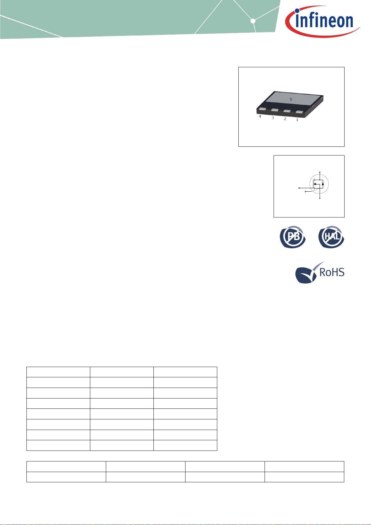
ThinPAK8x8
Drain
Pin 5
Gate
Pin 1
Power
Source
Pin 3,4
Driver
Source
Pin 2
MOSFET
600VCoolMOSªC7PowerTransistor
CoolMOS™C7isarevolutionarytechnologyforhighvoltagepower
MOSFETs,designedaccordingtothesuperjunction(SJ)principleand
pioneeredbyInfineonTechnologies.
600VCoolMOS™C7seriescombinestheexperienceoftheleadingSJ
MOSFETsupplierwithhighclassinnovation.
The600VC7isthefirsttechnologyeverwithR
DS(on)
*Abelow1Ohm*mm².
Features
•Suitableforhardandsoftswitching(PFCandhighperformanceLLC)
•IncreasedMOSFETdv/dtruggednessto120V/ns
•IncreasedefficiencyduetobestinclassFOMR
DS(on)
*E
oss
andR
DS(on)
*Q
g
•BestinclassR
DS(on)
/package
•SMDpackagewithverylowparasiticinductanceforeasydevicecontrol
•QualifiedforindustrialgradeapplicationsaccordingtoJEDEC(J-STD20
andJESD22)
•4pinkelvinsourceconcept
Benefits
•IncreasedeconomiesofscalebyuseinPFCandPWMtopologiesinthe
application
•Higherdv/dtlimitenablesfasterswitchingleadingtohigherefficiency
•Enablinghighersystemefficiencybylowerswitchinglosses
•Increasedpowerdensitysolutionsduetosmallerpackages
•OptimizedPCBassemblyandlayoutsolutions
•Suitableforapplicationssuchasserver,telecomandsolar
•Upto0.5%betterfullloadefficiency@100kHzcomparedtoconventional
3pinpackage
Potentialapplications
PFCstagesandPWMstages(TTF,LLC)forhighpower/performance
SMPSe.g.Computing,Server,Telecom,UPSandSolar.
Pleasenote:ForMOSFETparallelingtheuseofferritebeadsonthegate
orseparatetotempolesisgenerallyrecommended.
Table1KeyPerformanceParameters
Parameter Value Unit
V
DS
@ T
j,max
650 V
R
DS(on),max
125 mΩ
Q
g,typ
34 nC
I
D,pulse
66 A
I
D,continuous
@ T
j
<150°C 30 A
E
oss
@ 400V 4 µJ
Body diode di
F
/dt 380 A/µs
Type/OrderingCode Package Marking RelatedLinks
IPL60R125C7 PG-VSON-4 60C7125 see Appendix A


剩余13页未读,继续阅读
资源评论


芯脉芯城
- 粉丝: 4
- 资源: 4030


最新资源
- 【毕业设计】基于信誉共识和联邦学习的异构车联网交通预测与规划源码+项目说明.zip
- comsol 电化学仿真-PEMFC 低温质子交膜氨-氢燃料电池仿真和氢燃料电池,包含电化学-流场-浓度-温度-膜中水,参考一篇二区文章模型搭建
- 山东大学数据结构课设二叉树实现及分析
- Bongo cat mver 桌宠
- 汽车租赁系统 毕业设计 源码+数据库+论文(JAVA+SpringBoot+Vue.JS).zip
- 基于zynq的以太网传输工程教学 内容:这是一个框架 将fpga获得的数据通过dma存入ddr 再从处理器端将数据从ddr读取并通过千兆网传输给电脑 意义:作为一个开发框架 继续这个框架可以半天就能
- 【毕业设计】缺陷检测-基于深度学习实现的高效轮胎磨损+缺陷检测算法实现python源码.zip
- 汽车租赁系统业务管理子系统 SSM毕业设计 源码+数据库+论文(JAVA+SpringBoot+Vue.JS).zip
- 【毕业设计】汽车站售票管理系统设计源码.zip
- 【毕业设计】聊天室、websocket、socket.io设计源码.zip
- 【毕业设计】使用TensorRT部署BEVDet-ROS模型C++源码.zip
- 储能优化 模型预测控制MPC 微电网 优化调度 能量管理 MATLAB:基于模型预测算法的含储能微网双层能量管理模型 参考文献:A Two-layer Energy Management Sy
- 【毕业设计】使用streamlit部署yolov9目标检测模型python源码+运行说明.zip
- 【毕业设计】使用TensorRT+Cpp部署SuperPoint+SuperGlue算法模型源码+运行环境说明.zip
- 【毕业设计】使用TensorRT部署BEVDet模型C++源码.zip
- 【毕业设计】使用YOLOv9+DeepSort实现的目标跟踪算法python源码.zip
资源上传下载、课程学习等过程中有任何疑问或建议,欢迎提出宝贵意见哦~我们会及时处理!
点击此处反馈


