没有合适的资源?快使用搜索试试~ 我知道了~
BTS712N1 英飞凌芯片 INFINEON 中文版规格书手册 英飞凌芯片 INFINEON 中文版规格书手册.pdf
需积分: 5 0 下载量 68 浏览量
2023-07-05
09:48:24
上传
评论
收藏 1.32MB PDF 举报
温馨提示
试读
17页
BTS712N1 英飞凌芯片 INFINEON 中文版规格书手册 英飞凌芯片 INFINEON 中文版规格书手册
资源推荐
资源详情
资源评论
Automotive Power
Data Sheet
Rev 1.3, 2010-03-16
Smart High-Side Power Switch
PROFET BTS712N1
Data Sheet 2 Rev 1.3, 2010-03-16
Smart High-Side Power Switch
BTS712N1
S
mart
F
our
Ch
anne
l
Hi
g
h
s
id
e
P
ower
S
w
i
tc
h
Features
•
Overload protection
•
Current limitation
•
Short-circuit protection
•
Thermal shutdown
•
Overvoltage protection
(including load dump)
•
Fast demagnetization of inductive loads
•
Reverse battery protection
1
)
•
Undervoltage and overvoltage shutdown
with auto-restart and hysteresis
•
Open drain diagnostic output
• Open load detection in OFF-state
•
CMOS compatible input
•
Loss of ground and loss of V
bb
protection
•
Electrostatic discharge (ESD) protection
Application
•
µC compatible power switch with diagnostic feedback
for 12 V and 24 V DC grounded loads
•
All types of resistive, inductive and capacitive loads
•
Replaces electromechanical relays and discrete circuits
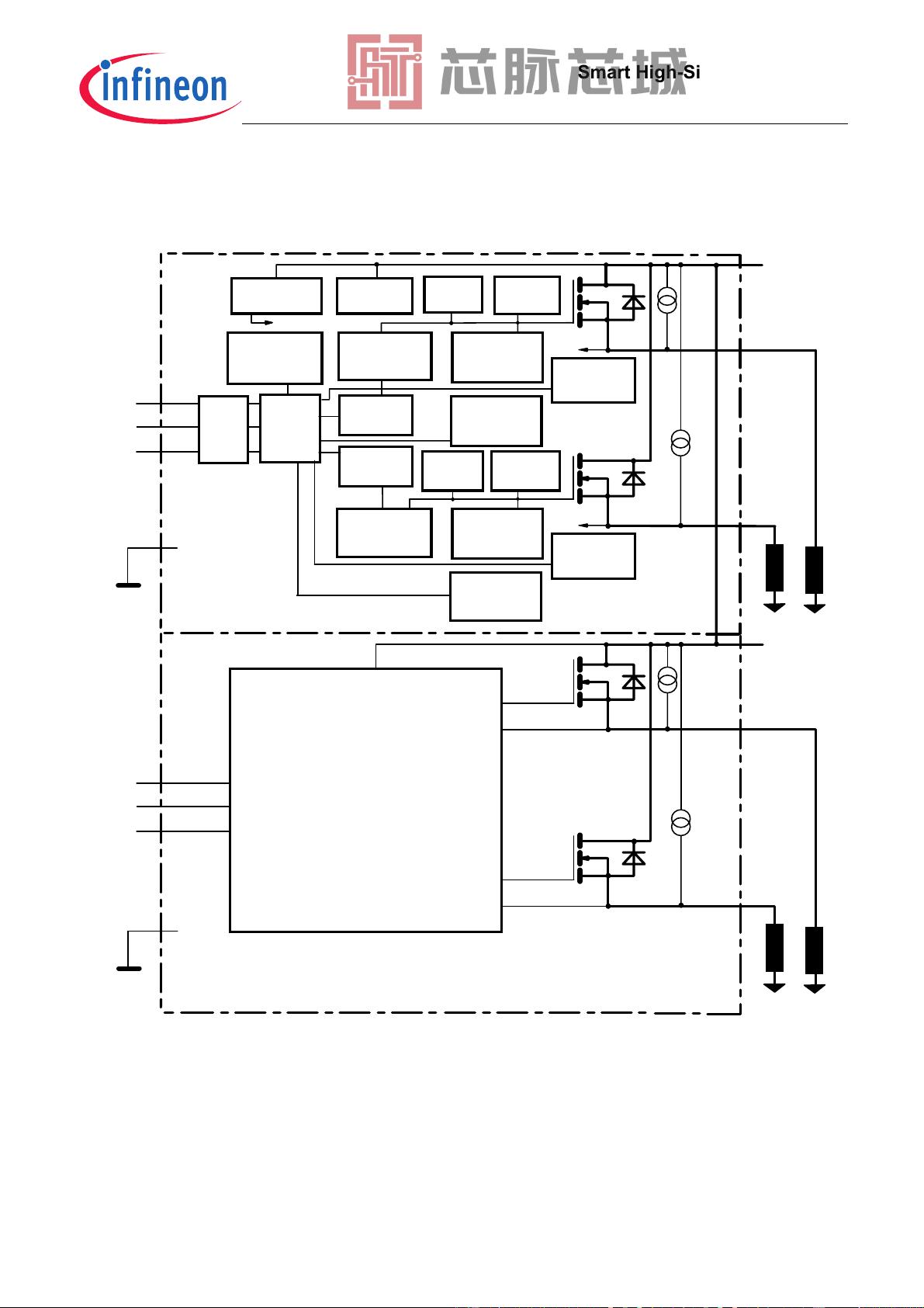
General Description
N channel vertical power FET with charge pump, ground referenced CMOS compatible input and diagnostic
feedback, monolithically integrated in Smart SIPMOS
technology.
Providing embedded protective functions.
Pin Definitions and Functions
Pin Symbol Function
1,10,
11,12,
15,16,
19,20
V
bb
Positive power supply voltage. Design the
wiring for the simultaneous max. short circuit
currents from channel 1 to 4 and also for low
thermal resistance
3 IN1 Input 1 .. 4, activates channel 1 .. 4 in case of
5 IN2 logic high signal
7 IN3
9 IN4
18 OUT1 Output 1 .. 4, protected high-side power output
17 OUT2 of channel 1 .. 4. Design the wiring for the
14 OUT3 max. short circuit current
13 OUT4
4 ST1/2 Diagnostic feedback 1/2 of channel 1 and
channel 2, open drain, low on failure
8 ST3/4 Diagnostic feedback 3/4 of channel 3 and
channel 4, open drain, low on failure
2 GND1/2 Ground 1/2 of chip 1 (channel 1 and channel 2)
6 GND3/4 Ground 3/4 of chip 2 (channel 3 and channel 4)
1)
With external current limit (e.g. resistor R
GND
=150 Ω) in GND connection, resistor in series with ST
connection, reverse load current limited by connected load.
Product Summary
Overvoltage Protection
V
bb(AZ)
43 V
Operating voltage
V
bb(on)
5.0 ... 34 V
active channels: one
two parallel four parallel
On-state resistance R
ON
200 100 50
mΩ
Nominal load current ,
/120
1.9 2.8 4.4 A
Current limitation ,
/6&U
4 4 4 A
Pin configuration (top view)
V
bb
1
•
20 V
bb
GND1/2 2 19 V
bb
IN1 3 18 OUT1
ST1/2 4 17 OUT2
IN2 5 16 V
bb
GND3/4 6 15 V
bb
IN3 7 14 OUT3
ST3/4 8 13 OUT4
IN4 9 12 V
bb
V
bb
10 11 V
bb
P-DSO-20
PG-DSO20
Data Sheet 3 Rev 1.3, 2010-03-16
Smart High-Side Power Switch
BTS712N1
Block diagram
Four Channels; Open Load detection in off state;
9
EE
,1
67
(6'
287
/RJLF
9ROWDJH
VHQVRU
9ROWDJH
VRXUFH
2SHQORDG
GHWHFWLRQ
6KRUWWR9EE
/HYHOVKLIWHU
7HPSHUDWXUH
VHQVRU
5HFWLILHU
/LPLWIRU
XQFODPSHG
LQGORDGV
*DWH
SURWHFWLRQ
&XUUHQW
OLPLW
9
/RJLF
2YHUYROWDJH
SURWHFWLRQ
287
2SHQORDG
GHWHFWLRQ
6KRUWWR9EE
/HYHOVKLIWHU
7HPSHUDWXUH
VHQVRU
5HFWLILHU
/LPLWIRU
XQFODPSHG
LQGORDGV
*DWH
SURWHFWLRQ
&XUUHQW
OLPLW
,1
&KDUJH
SXPS
&KDUJH
SXPS
&KDQQHO
&KDQQHO
6LJQDO*1'
*1'
&KLS
&KLS
9
EE
,1
67
352)(7
287
287
,1
&KDQQHO
&KDQQHO
/HDGIUDPHFRQQHFWHGWRSLQ
/HDGIUDPH
/RDG*1'
/RDG
/HDGIUDPH
/RDG*1'
/RDG
6LJQDO*1'
*1'
&KLS
&KLS
/RJLFDQGSURWHFWLRQFLUFXLWRIFKLS
HTXLYDOHQWWRFKLS
Data Sheet 4 Rev 1.3, 2010-03-16
Smart High-Side Power Switch
BTS712N1
Maximum Ratings at
T
j
= 25°C unless otherwise specified
Parameter Symbol Values Unit
Supply voltage (overvoltage protection see page 4)
V
bb
43 V
Supply voltage for full short circuit protection
T
j,start
=-40 ...+150°C
V
bb
34 V
Load current (Short-circuit current, see page 5)
I
L
self-limited A
Load dump protection
2)
V
LoadDump
=
U
A
+
V
s
,
U
A
= 13.5 V
R
I
3)
= 2 Ω,
t
d
= 200 ms; IN = low or high,
each channel loaded with
R
L
= 7.1 Ω,
V
Load
dump
4
)
60 V
Operating temperature range
Storage temperature range
T
j
T
stg
-40 ...+150
-55 ...+150
°C
Power dissipation (DC)
5
T
a
= 25°C:
(all channels active)
T
a
= 85°C:
P
tot
3.6
1.9
W
Inductive load switch-off energy dissipation, single pulse
V
bb
=12V,
T
j,start
=150°C
5)
,
I
L
= 1.9 A, Z
L
= 66 mH, 0Ω one channel:
I
L
= 2.8 A, Z
L
= 66 mH, 0Ω two parallel channels:
I
L
= 4.4 A, Z
L
= 66 mH, 0Ω four parallel channels:
see diagrams on page 9
E
AS
150
320
800
mJ
Electrostatic discharge capability (ESD)
(Human Body Model)
V
ESD
1.0 kV
Input voltage (DC)
V
IN
-10 ... +16 V
Current through input pin (DC)
Current through status pin (DC)
see internal circuit diagram page 8
I
IN
I
ST
±2.0
±5.0
mA
Thermal resistance
junction - soldering point
5),6)
each channel:
R
thjs
16 K/W
junction - ambient
5)
one channel active:
all channels active:
R
thja
44
35
2)
Supply voltages higher than V
bb(AZ)
require an external current limit for the GND and status pins, e.g. with a
150 Ω resistor in the GND connection and a 15 kΩ resistor in series with the status pin. A resistor for input
protection is integrated.
3)
R
I
= internal resistance of the load dump test pulse generator
4)
V
Load dump
is setup without the DUT connected to the generator per ISO 7637-1 and DIN 40839
5)
Device on 50mm*50mm*1.5mm epoxy PCB FR4 with 6cm
2
(one layer, 70µm thick) copper area for V
bb
co
nn
ect
i
o
n. P
C
B i
s
v
e
r
t
i
ca
l wi
t
h
out
b
l
o
wn
a
ir.
See
page
14
剩余16页未读,继续阅读
资源评论
芯脉芯城
- 粉丝: 3
- 资源: 4031
上传资源 快速赚钱
- 我的内容管理 展开
- 我的资源 快来上传第一个资源
- 我的收益 登录查看自己的收益
- 我的积分 登录查看自己的积分
- 我的C币 登录后查看C币余额
- 我的收藏
- 我的下载
- 下载帮助
安全验证
文档复制为VIP权益,开通VIP直接复制
信息提交成功