IPL60R105P7 INFINEON 英飞凌芯片 中文版规格书手册.pdf
需积分: 5 105 浏览量
2023-06-09
11:07:20
上传
评论
收藏 1.35MB PDF 举报

1
IPL60R105P7
Rev.2.1,2018-05-15Final Data Sheet
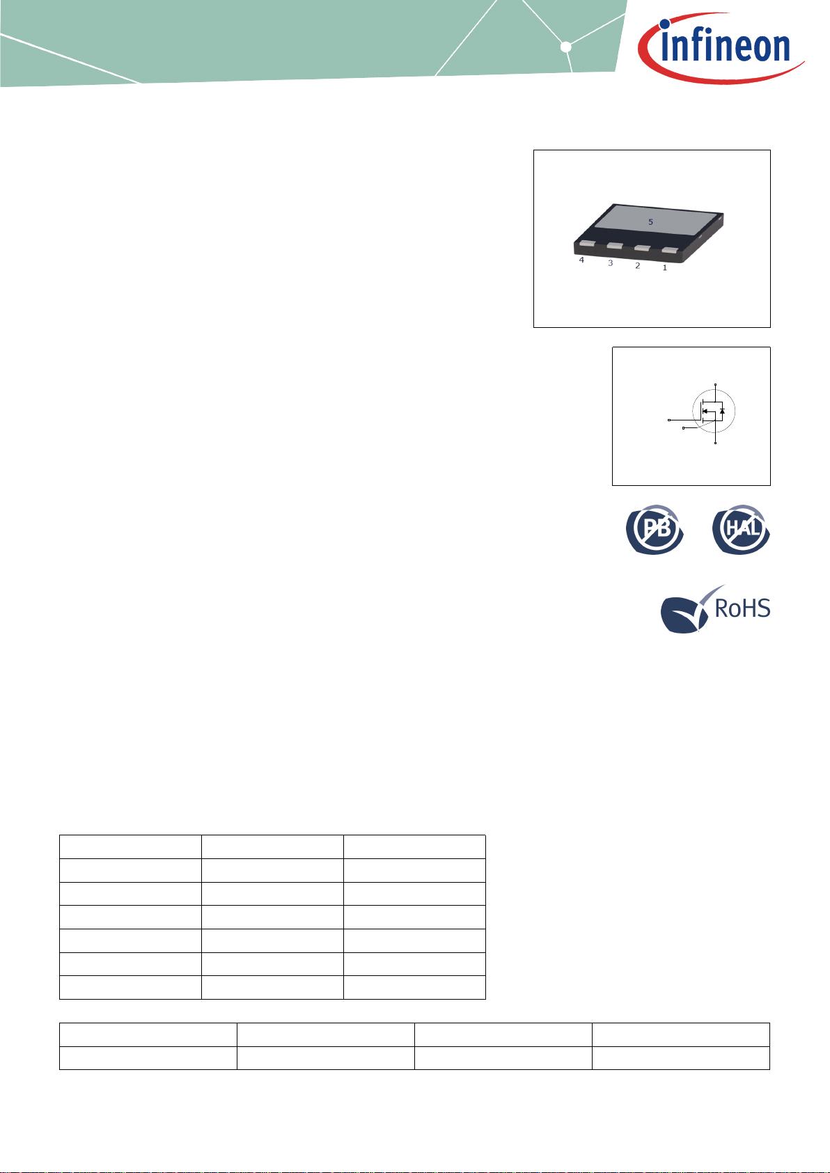
ThinPAK8x8
Drain
Pin 5
Gate
Pin 1
Power
Source
Pin 3,4
Driver
Source
Pin 2
MOSFET
600VCoolMOSªP7PowerTransistor
TheCoolMOS™7thgenerationplatformisarevolutionarytechnologyfor
highvoltagepowerMOSFETs,designedaccordingtothesuperjunction
(SJ)principleandpioneeredbyInfineonTechnologies.The600V
CoolMOS™P7seriesisthesuccessortotheCoolMOS™P6series.It
combinesthebenefitsofafastswitchingSJMOSFETwithexcellentease
ofuse,e.g.verylowringingtendency,outstandingrobustnessofbody
diodeagainsthardcommutationandexcellentESDcapability.
Furthermore,extremelylowswitchingandconductionlossesmake
switchingapplicationsevenmoreefficient,morecompactandmuch
cooler.
Features
•Suitableforhardandsoftswitching(PFCandLLC)duetoanoutstanding
commutationruggedness
•Significantreductionofswitchingandconductionlosses
•ExcellentESDrobustness>2kV(HBM)forallproducts
•BetterR
DS(on)
/packageproductscomparedtocompetitionenabledbya
lowR
DS(on)
*A(below1Ohm*mm²)
•Fullyqualifiedacc.JEDECforIndustrialApplications
Benefits
•Easeofuseandfastdesign-inthroughlowringingtendencyandusage
acrossPFCandPWMstages
•Simplifiedthermalmanagementduetolowswitchingandconduction
losses
•Increasedpowerdensitysolutionsenabledbyusingproductswith
smallerfootprintandhighermanufacturingqualitydueto>2kVESD
protection
•Suitableforawidevarietyofapplicationsandpowerranges
Potentialapplications
PFCstages,hardswitchingPWMstagesandresonantswitchingstages
fore.g.PCSilverbox,Adapter,LCD&PDPTV,Lighting,Server,Telecom
andUPS.
Pleasenote:ForMOSFETparallelingtheuseofferritebeadsonthegate
orseparatetotempolesisgenerallyrecommended.
Table1KeyPerformanceParameters
Parameter Value Unit
V
DS
@ T
j,max
650 V
R
DS(on),max
105 mΩ
Q
g,typ
45 nC
I
D,pulse
100 A
E
oss
@ 400V 5.0 µJ
Body diode di
F
/dt 800 A/µs
Type/OrderingCode Package Marking RelatedLinks
IPL60R105P7 PG-VSON-4 60R105P7 see Appendix A


剩余13页未读,继续阅读
资源评论


芯脉芯城
- 粉丝: 3
- 资源: 4031


最新资源
- 以下是一些适用于英语六级作文的万能句型模板,涵盖了引言、正文和结论部分的各类表达方式.docx
- MATLAB中的非线性规划
- 进行C语言面试资格确认是招聘过程中一个重要的步骤,目的是确保候选人具备足够的C语言编程能力和知识.docx
- Java 轻量级的集群负载均衡设计
- 纹身师个人网站模板.jpg
- 在C语言中,连接两个字符串(即将一个字符串附加到另一个字符串的末尾)通常可以使用标准库中的 `strcat` 函数.docx
- 数据库管理工具:dbeaver-ce-23.1.1-stable.x86-64.rpm
- 以下是几个具体竞赛题目的详细解答,包括建模思路、方法和步骤 .docx
- 一份关于全国大学生建模大赛的相关教程!!
- 以下是关于计算机网络和现代通信组网的详细教程、案例和相关项目的推荐.docx
资源上传下载、课程学习等过程中有任何疑问或建议,欢迎提出宝贵意见哦~我们会及时处理!
点击此处反馈


