没有合适的资源?快使用搜索试试~ 我知道了~
TI-CD74AC157.pdf
需积分: 10 0 下载量 17 浏览量
2022-11-29
13:03:12
上传
评论 4
收藏 943KB PDF 举报
温馨提示
试读
14页
TI-CD74AC157.pdf
资源推荐
资源详情
资源评论
CD54AC157, CD74AC157
QUADRUPLE 2-LINE TO 1-LINE DATA SELECTORS/MULTIPLEXERS
SCHS335 – MARCH 2003
1
POST OFFICE BOX 655303 • DALLAS, TEXAS 75265
D
AC Types Feature 1.5-V to 5.5-V Operation
and Balanced Noise Immunity at 30% of the
Supply Voltage
D
Speed of Bipolar F, AS, and S, With
Significantly Reduced Power Consumption
D
Balanced Propagation Delays
D
±24-mA Output Drive Current
– Fanout to 15 F Devices
D
SCR-Latchup-Resistant CMOS Process and
Circuit Design
D
Exceeds 2-kV ESD Protection Per
MIL-STD-883, Method 3015
description/ordering information
These quadruple 2-line to 1-line data selectors/multiplexers are designed for 1.5-V to 5.5-V V
CC
operation.
The ’AC157 devices feature a common strobe (G
) input. When the strobe is high, all outputs are low. When the
strobe is low, a 4-bit word is selected from one of two sources and is routed to the four outputs. The devices
provide true data.
ORDERING INFORMATION
T
A
PACKAGE
†
ORDERABLE
PART NUMBER
TOP-SIDE
MARKING
PDIP – E Tube CD74AC157E CD74AC157E
55°Cto125°C
SOIC M
Tube CD74AC157M
AC157M
–
55°C
to
125°C
SOIC
–
M
Tape and reel CD74AC157M96
AC157M
CDIP – F Tube CD54AC157F3A CD54AC157F3A
†
Package drawings, standard packing quantities, thermal data, symbolization, and PCB design guidelines
are available at www.ti.com/sc/package.
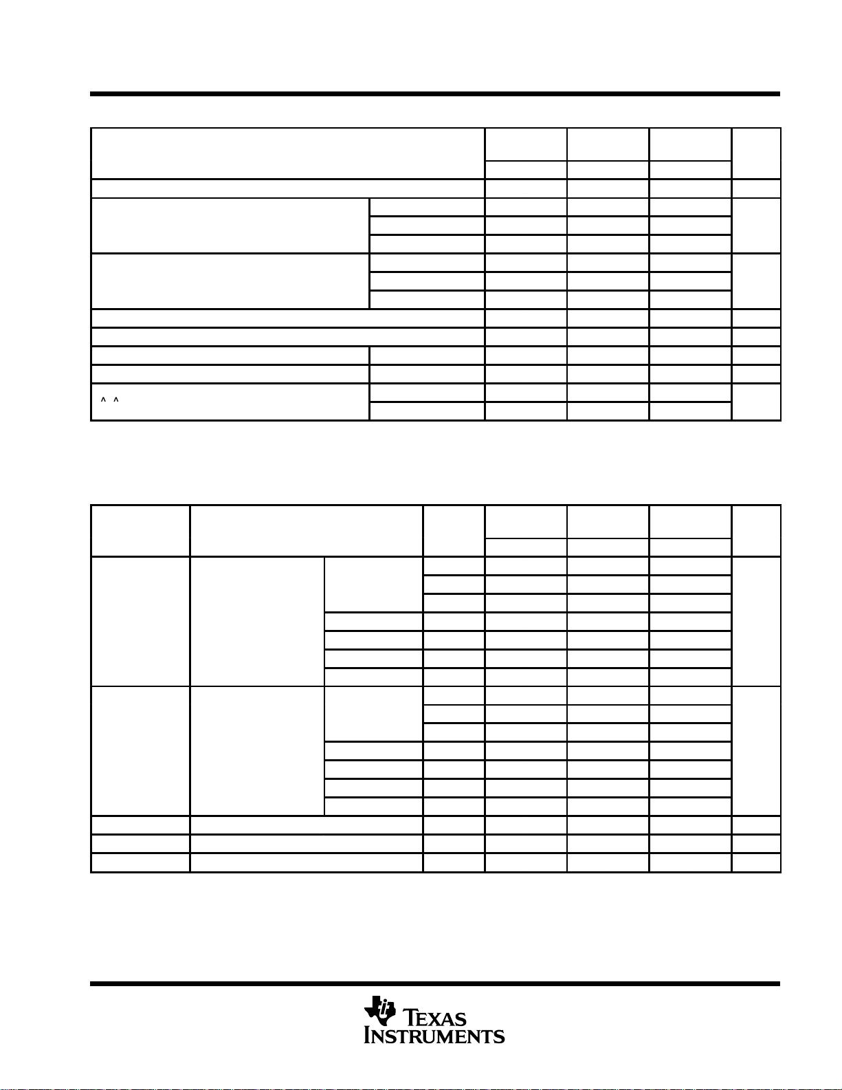
FUNCTION TABLE
INPUTS
OUTPUT
G A/B A B
Y
H X X X L
L LLX L
L LHX H
L HXL L
L H X H H
Copyright 2003, Texas Instruments Incorporated
PRODUCTION DATA information is current as of publication date.
Products conform to specifications per the terms of Texas Instruments
standard warranty. Production processing does not necessarily include
testing of all parameters.
Please be aware that an important notice concerning availability, standard warranty, and use in critical applications of
Texas Instruments semiconductor products and disclaimers thereto appears at the end of this data sheet.
1
2
3
4
5
6
7
8
16
15
14
13
12
11
10
9
A/B
1A
1B
1Y
2A
2B
2Y
GND
V
CC
G
4A
4B
4Y
3A
3B
3Y
CD54AC157 ...F PACKAGE
CD74AC157 ...E OR M PACKAGE
(TOP VIEW)
On products compliant to MIL-PRF-38535, all parameters are tested
unless otherwise noted. On all other products, production
processing does not necessarily include testing of all parameters.
CD54AC157, CD74AC157
QUADRUPLE 2-LINE TO 1-LINE DATA SELECTORS/MULTIPLEXERS
SCHS335 – MARCH 2003
2
POST OFFICE BOX 655303 • DALLAS, TEXAS 75265
logic diagram (positive logic)
2
3
5
6
11
10
14
13
15
1
G
A/B
4B
4A
3B
3A
2B
2A
1B
1A
4
7
9
12
1Y
2Y
3Y
4Y
absolute maximum ratings over operating free-air temperature range (unless otherwise noted)
†
Supply voltage range, V
CC
–0.5 V to 6 V. . . . . . . . . . . . . . . . . . . . . . . . . . . . . . . . . . . . . . . . . . . . . . . . . . . . . . . . . .
Input clamp current, I
IK
(V
I
< 0 V or V
I
> V
CC
) (see Note 1) ±20 mA. . . . . . . . . . . . . . . . . . . . . . . . . . . . . . . . . . .
Output clamp current, I
OK
(V
O
< 0 V or V
O
> V
CC
) (see Note 1) ±50 mA. . . . . . . . . . . . . . . . . . . . . . . . . . . . . .
Continuous output current, I
O
(V
O
> 0 V or V
O
< V
CC
) ±50 mA. . . . . . . . . . . . . . . . . . . . . . . . . . . . . . . . . . . . . . .
Continuous current through V
CC
or GND ±100 mA. . . . . . . . . . . . . . . . . . . . . . . . . . . . . . . . . . . . . . . . . . . . . . . . . .
Package thermal impedance, θ
JA
(see Note 2): E package 67°C/W. . . . . . . . . . . . . . . . . . . . . . . . . . . . . . . . . . .
M package 73°C/W. . . . . . . . . . . . . . . . . . . . . . . . . . . . . . . . . .
Storage temperature range, T
stg
–65°C to 150°C. . . . . . . . . . . . . . . . . . . . . . . . . . . . . . . . . . . . . . . . . . . . . . . . . . .
†
Stresses beyond those listed under “absolute maximum ratings” may cause permanent damage to the device. These are stress ratings only, and
functional operation of the device at these or any other conditions beyond those indicated under “recommended operating conditions” is not
implied. Exposure to absolute-maximum-rated conditions for extended periods may affect device reliability.
NOTES: 1. The input and output voltage ratings may be exceeded if the input and output current ratings are observed.
2. The package thermal impedance is calculated in accordance with JESD 51-7.
CD54AC157, CD74AC157
QUADRUPLE 2-LINE TO 1-LINE DATA SELECTORS/MULTIPLEXERS
SCHS335 – MARCH 2003
3
POST OFFICE BOX 655303 • DALLAS, TEXAS 75265
recommended operating conditions (see Note 3)
T
A
= 25°C
–55°C to
125°C
–40°C to
85°C
UNIT
MIN MAX MIN MAX MIN MAX
V
CC
Supply voltage 1.5 5.5 1.5 5.5 1.5 5.5 V
V
CC
= 1.5 V 1.2 1.2 1.2
V
IH
High-level input voltage
V
CC
= 3 V
2.1 2.1 2.1
V
V
CC
= 5.5 V 3.85 3.85 3.85
V
CC
= 1.5 V 0.3 0.3 0.3
V
IL
Low-level input voltage
V
CC
= 3 V
0.9 0.9 0.9
V
V
CC
= 5.5 V 1.65 1.65 1.65
V
I
Input voltage 0 V
CC
0 V
CC
0 V
CC
V
V
O
Output voltage 0 V
CC
0 V
CC
0 V
CC
V
I
OH
High-level output current V
CC
= 4.5 V to 5.5 V –24 –24 –24 mA
I
OL
Low-level output current V
CC
= 4.5 V to 5.5 V 24 24 24 mA
∆t/∆v
In
p
ut transition rise or fall rate
V
CC
= 1.5 V to 3 V 50 50 50
ns/V
∆t/∆v
Input
transition
rise
or
fall
rate
V
CC
= 3.6 V to 5.5 V 20 20 20
ns/V
NOTE 3: All unused inputs of the device must be held at V
CC
or GND to ensure proper device operation. Refer to the TI application report,
Implications of Slow or Floating CMOS Inputs, literature number SCBA004.
electrical characteristics over recommended operating free-air temperature range (unless
otherwise noted)
PARAMETER TEST CONDITIONS V
CC
T
A
= 25°C
–55°C to
125°C
–40°C to
85°C
UNIT
CC
MIN MAX MIN MAX MIN MAX
1.5 V 1.4 1.4 1.4
I
OH
= –50 µA
3 V 2.9 2.9 2.9
4.5 V 4.4 4.4 4.4
V
OH
V
I
= V
IH
or V
IL
I
OH
= –4 mA 3 V 2.58 2.4 2.48
V
I
OH
= –24 mA 4.5 V 3.94 3.7 3.8
I
OH
= –50 mA
†
5.5 V 3.85
I
OH
= –75 mA
†
5.5 V 3.85
1.5 V 0.1 0.1 0.1
I
OL
= 50 µA
3 V 0.1 0.1 0.1
4.5 V 0.1 0.1 0.1
V
OL
V
I
= V
IH
or V
IL
I
OL
= 12 mA 3 V 0.36 0.5 0.44
V
I
OL
= 24 mA 4.5 V 0.36 0.5 0.44
I
OL
= 50 mA
†
5.5 V 1.65
I
OL
= 75 mA
†
5.5 V 1.65
I
I
V
I
= V
CC
or GND 5.5 V ±0.1 ±1 ±1 µA
I
CC
V
I
= V
CC
or GND, I
O
= 0 5.5 V 8 160 80 µA
C
i
10 10 10 pF
†
Test one output at a time, not exceeding 1-second duration. Measurement is made by forcing indicated current and measuring voltage to minimize
power dissipation. Test verifies a minimum 50-Ω transmission-line drive capability at 85°C and 75-Ω transmission-line drive capability at 125°C.
剩余13页未读,继续阅读
资源评论
不觉明了
- 粉丝: 3195
- 资源: 5518
上传资源 快速赚钱
- 我的内容管理 展开
- 我的资源 快来上传第一个资源
- 我的收益 登录查看自己的收益
- 我的积分 登录查看自己的积分
- 我的C币 登录后查看C币余额
- 我的收藏
- 我的下载
- 下载帮助
安全验证
文档复制为VIP权益,开通VIP直接复制
信息提交成功