TI-TPS51216-EP.pdf
需积分: 9 36 浏览量
2022-11-20
17:25:12
上传
评论 5
收藏 1.47MB PDF 举报

12
17
16
6
15
14
13
11
V5IN
TPS51216
S3
S5
VREF
VBST
DRVH
SW
DRVL
8
10
REFIN
PGND
7
19
GND
MODE
18 TRIP
20
9
2
3
PGOOD
VDDQSNS
VLDOIN
VTT
1
4
5
VTTSNS
VTTGND
VTTREF
UDG-10138
VDDQ
VTT
PGND
S3
S5
PGND
5VIN
PGND
VIN
VTTREF
AGND
AGND
Powergood
Product
Folder
Sample &
Buy
Technical
Documents
Tools &
Software
Support &
Community
TPS51216-EP
SLUSCA7 –NOVEMBER 2015
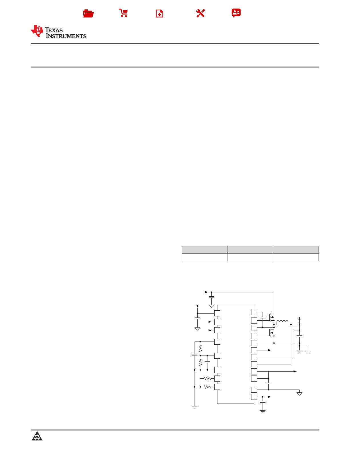
TPS51216-EP Complete DDR2, DDR3 and DDR3L Memory Power Solution Synchronous
Buck Controller, 2-A LDO, Buffered Reference
1 Features 2 Applications
1
• Synchronous Buck Controller (VDDQ)
• DDR2/DDR3/DDR3L Memory Power Supplies
• SSTL_18, SSTL_15, SSTL_135, and HSTL
– Conversion Voltage Range: 3 to 28 V
Termination
– Output Voltage Range: 0.7 to 1.8 V
– 0.8% V
REF
Accuracy
3 Description
– D-CAP™ Mode for Fast Transient Response
The TPS51216-EP provides a complete power supply
– Selectable 300-kHz/400-kHz Switching
for DDR2, DDR3 and DDR3L memory systems in the
Frequencies
lowest total cost and minimum space. It integrates a
synchronous buck regulator controller (VDDQ) with a
– Optimized Efficiency at Light and Heavy Loads
2-A sink/source tracking LDO (VTT) and buffered low
With Auto-Skip Function
noise reference (VTTREF). The TPS51216-EP
– Supports Soft-Off in S4/S5 States
employs D-CAP™ mode coupled with 300 kHz/400
– OCL/OVP/UVP/UVLO Protections
kHz frequencies for ease-of-use and fast transient
response. The VTTREF tracks VDDQ/2 within
– Powergood Output
excellent 0.8% accuracy. The VTT, which provides 2-
• 2-A LDO (VTT), Buffered Reference (VTTREF)
A sink/source peak current capabilities, requires only
– 2-A (Peak) Sink and Source Current
10-μF of ceramic capacitance. In addition, a
dedicated LDO supply input is available.
– Requires Only 10-μF of Ceramic Output
Capacitance
The TPS51216-EP provides rich useful functions as
– Buffered, Low Noise, 10-mA VTTREF Output
well as excellent power supply performance. It
supports flexible power state control, placing VTT at
– 0.8% VTTREF, 20-mV VTT Accuracy
high-Z in S3 and discharging VDDQ, VTT, and
– Support High-Z in S3 and Soft-Off in S4/S5
VTTREF (soft-off) in S4/S5 state.
• Thermal Shutdown
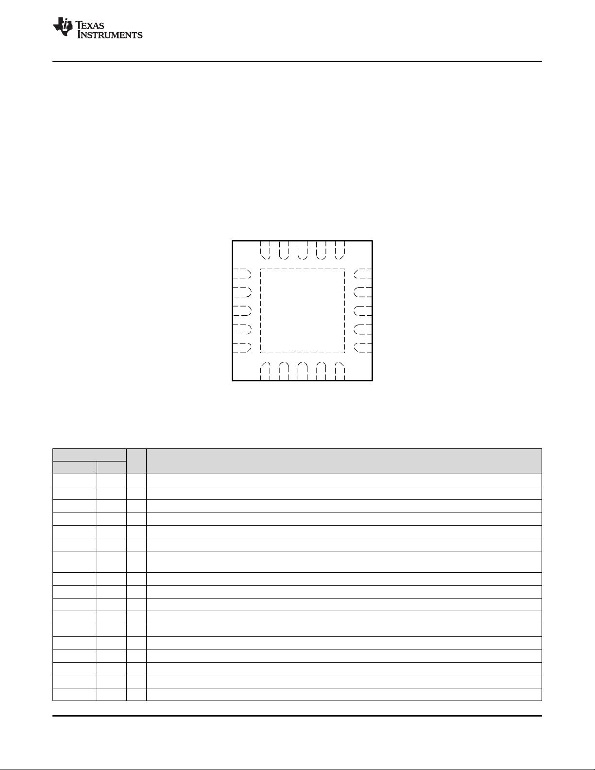
Device Information
(1)
• 20-Pin, 3 mm × 3 mm, WQFN Package
PART NUMBER PACKAGE BODY SIZE (NOM)
• Supports Defense, Aerospace, and Medical
TPS51216-EP WQFN (20) 3.00 mm × 3.00 mm
Applications
(1) For all available packages, see the orderable addendum at
– Controlled Baseline
the end of the data sheet.
– One Assembly/Test Site
– One Fabrication Site
Application Diagram
– Available in Military (–55°C to 125°C)
Temperature Range
(1)
– Extended Product Life Cycle
– Extended Product-Change Notification
– Product Traceability
(1) Additional temperature ranges available - contact factory
1
An IMPORTANT NOTICE at the end of this data sheet addresses availability, warranty, changes, use in safety-critical applications,
intellectual property matters and other important disclaimers. PRODUCTION DATA.

剩余33页未读,继续阅读
资源评论


