TI-TPS51200-EP.pdf
需积分: 10 185 浏览量
2022-11-20
17:26:09
上传
评论 5
收藏 1.26MB PDF 举报

2
3
4
5
1
9
8
7
6
10
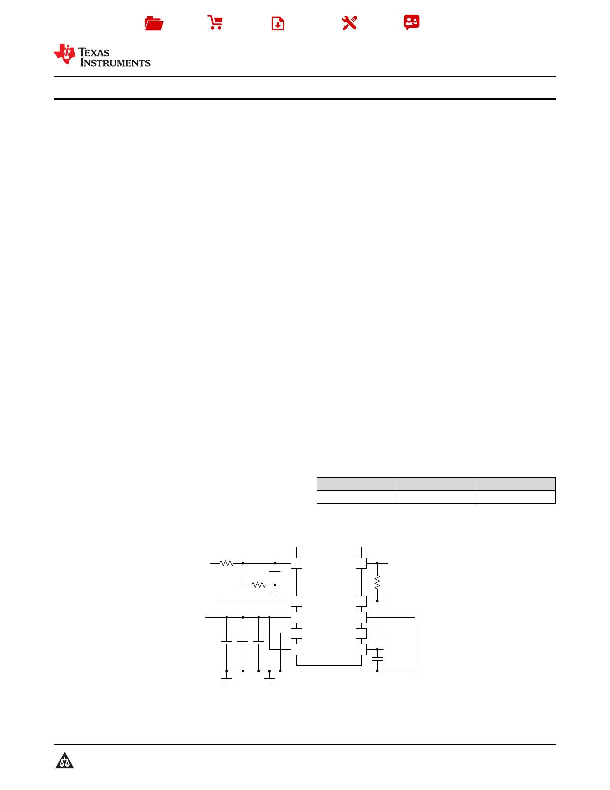
TPS51200
REFIN
VLDOIN
VO
PGND
VOSNS
VIN
PGOOD
GND
EN
REFOUT
3.3 V
IN
PGOOD
SLP_S3
VTTREF
VLDOIN
V
TT
V
DDQ
Copyright © 2016, Texas Instruments Incorporated
Product
Folder
Sample &
Buy
Technical
Documents
Tools &
Software
Support &
Community
An IMPORTANT NOTICE at the end of this data sheet addresses availability, warranty, changes, use in safety-critical applications,
intellectual property matters and other important disclaimers. PRODUCTION DATA.
English Data Sheet: SLUSA48
TPS51200-EP
ZHCSF57 –JUNE 2016
TPS51200-EP 灌灌/拉拉 DDR 终终端端稳稳压压器器
1
1 特特性性
1
• 输入电压:支持 2.5V 和 3.3V 电源轨
• VLDOIN 电压范围:1.1V 至 3.5V
• 具有压降补偿功能的灌电流和拉电流终端稳压器
• 所需最小输出电容为 20μF(通常为 3 × 10μF
MLCC),用于存储器终端 应用 (DDR)
• 用于监视输出稳压的 PGOOD
• EN 输入
• REFIN 输入允许直接或通过电阻分压器灵活进行输
入跟踪
• 远程感测 (VOSNS)
• ±10mA 缓冲基准 (REFOUT)
• 内置软启动,欠压锁定 (UVLO) 和过流限制 (OCL)
• 热关断
• 符合 DDR 和 DDR2 JEDEC 规范
• 支持 DDR3、低功耗 DDR3 和 DDR4 VTT 应用
• 带有散热焊盘的 10 引脚超薄小外形尺寸无引线
(VSON) 封装
• 支支持持国国防防、、航航天天和和医医疗疗 应应用用
– 受控基线
– 一个组装和测试场所
– 一个制造场所
– 支持军用温度范围(-55°C 至 125°C)
– 延长的产品使用寿命周期
– 延长的产品变更通知
– 产品可追溯性
2 应应用用范范围围
• 用于 DDR、DDR2、DDR3、低功耗 DDR3 和
DDR4 的存储器终端稳压器
• 笔记本、台式机和服务器
• 电信和数据通信
• 基站
• 液晶 (LCD) 电视和等离子 (PDP) 电视
• 复印机和打印机
• 机顶盒
3 说说明明
TPS51200-EP 器件是一款灌电流和拉电流双倍数据速
率 (DDR) 终端稳压器,专用于空间问题是重要考量因
素的低输入电压、低成本、低噪声系统。
TPS51200-EP 能够保持快速瞬态响应,最低仅需
20μF 输出电容。TPS51200-EP 支持远程感测功能并
且可满足 DDR、DDR2、DDR3、低功耗 DDR3 和
DDR4 VTT 总线的所有电源要求。
此外,TPS51200-EP 还提供一个开漏 PGOOD 信号
监测输出稳压,提供一个 EN 信号在 S3(挂起至
RA4M)期间针对 DDR 进行 VTT 放电。
TPS51200-EP 采用带散热焊盘的高效散热型 10 引脚
超薄小外形尺寸无引线 (VSON) 封装,无铅且绿色环
保。其额定工作温度范围为 -55°C 至 +125°C。
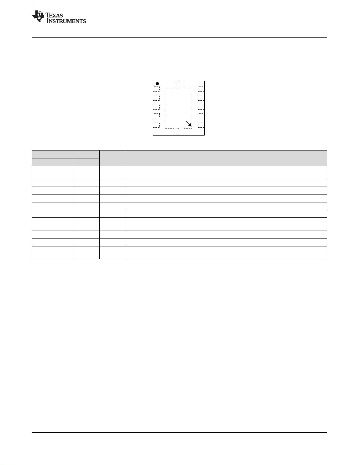
器器件件信信息息
(1)
器器件件型型号号 封封装装 封封装装尺尺寸寸((标标称称值值))
TPS51200-EP VSON (10) 3.00mm x 3.00mm
(1) 要了解所有可用封装,请见数据表末尾的可订购产品附录。
简简化化的的 DDR 应应用用

剩余36页未读,继续阅读
资源评论


