TI-TPS55340-EP.pdf
需积分: 8 132 浏览量
2022-10-24
22:57:12
上传
评论 5
收藏 2.51MB PDF 举报

TPS55340-EP 集成式 5A、40V 宽输入范围
升压/SEPIC/反激式直流/直流稳压器
1 特性
• 内部 5A,40V 低侧 MOSFET 开关
• 2.9V 至 32V 输入电压范围
• ±0.7% 基准电压
• 0.5mA 静态工作电流
• 2.7µA 关断电源电流
• 固定频率电流模式脉宽调制 (PWM) 控制
• 频率可在 100kHz 至 1.2MHz 之间调整
• 同步外部时钟功能
• 软启动时间可调节
• 用于在轻负载时实现较高效率的脉冲跳跃模式
• 逐周期电流限制、热关断和 UVLO 保护
• 支持国防、航天和医疗应用
– 受控基线
– 一个组装和测试基地
– 一个制造基地
– 支持军用(–55°C 至 125°C)温度范围
– 延长了产品生命周期
– 延长了产品变更通知
– 产品可追溯性
2 应用
• 3.3V、5V、12V、24V 功率转换
• 升压、SEPIC 和反激式拓扑结构
• 适用于平板电脑和便携式个人电脑的 Thunderbolt
端口、电源扩展坞
• 工业电源系统
• ADSL 调制解调器
3 说明
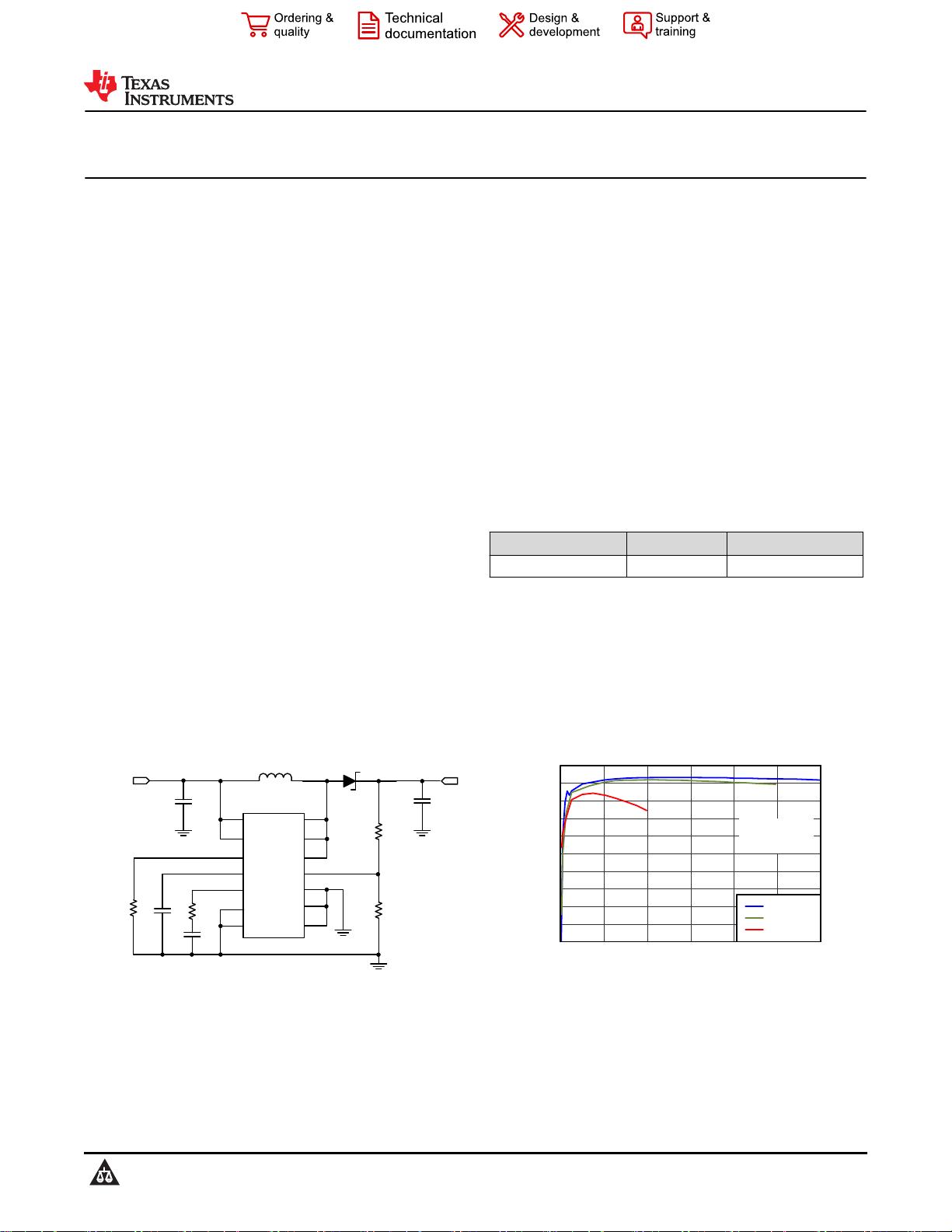
TPS55340-EP 是一款单片非同步开关稳压器,带有集
成的 5A/40V 电源开关。此器件可配置成多种标准开关
稳压器拓扑,包括升压、SEPIC 和隔离反激式。此器
件具有宽输入电压范围,可支持输入电压来自多节电池
或者稳压的 3.3V、5V、12V 和 24V 电源轨的应用。
TPS55340-EP 使用电流模式脉宽调制 (PWM) 控制来
调节输出电压,并具有一个内部振荡器。PWM 的开关
频率由一个外部电阻器设定或者通过与一个外部时钟信
号同步来设置。用户可以在 100kHz 至 1.2MHz 之间
对开关频率进行设定。
此器件具有可编程软启动功能,可限制启动期间的涌入
电流,并且还具有其他内置保护特性,包括逐周期过流
限制和热关断。
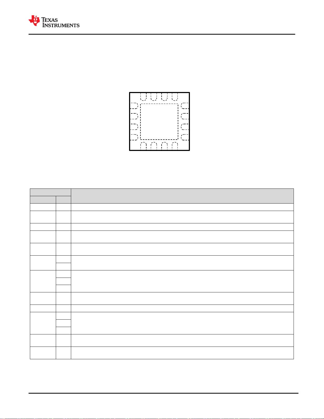
器件信息
订货编号
封装
(1)
封装尺寸(标称值)
TPS55340MRTETEP WQFN (16) 3.00mm × 3.00mm
(1) 要了解所有可用封装,请见数据表末尾的可订购产品附录。
TPS55340
VIN
EN
SW
SW
SW
FREQ
SS
COMP
SYNC
FB
PGND
PGND
PGND
V
IN
V
OUT
R
SL
R
SH
L
D
C
I
C
O
R
FREQ
C
SS
R
C
C
C
AGND
典型应用(升压)
50
55
60
65
70
75
80
85
90
95
100
0 0.4 0.8 1.2 1.6 2 2.4
Output Current (A)
Efficiency (%)
V
IN
= 15 V
V
IN
= 12 V
V
IN
= 5 V
V
OUT
= 24 V
f
SW
= 600 kHz
G031
效率与输出电流间的关系
TPS55340-EP
ZHCSCL9A – JULY 2014 – REVISED SEPTEMBER 2021
本文档旨在为方便起见,提供有关 TI 产品中文版本的信息,以确认产品的概要。有关适用的官方英文版本的最新信息,请访问
www.ti.com,其内容始终优先。TI 不保证翻译的准确性和有效性。在实际设计之前,请务必参考最新版本的英文版本。
English Data Sheet: SLVSCG7

剩余39页未读,继续阅读
资源评论


