没有合适的资源?快使用搜索试试~ 我知道了~
TI-TPS71202-EP.pdf
需积分: 9 0 下载量 90 浏览量
2022-10-28
23:50:52
上传
评论 5
收藏 1.41MB PDF 举报
温馨提示
试读
20页
TI-TPS71202-EP.pdf
资源推荐
资源详情
资源评论
TPS71202-EP
www.ti.com
SGLS395A –OCTOBER 2008–REVISED SEPTEMBER 2010
DUAL, 250-mA OUTPUT, ULTRA-LOW NOISE, HIGH PSRR, LOW-DROPOUT
LINEAR REGULATOR
Check for Samples: TPS71202-EP
1
FEATURES
SUPPORTS DEFENSE, AEROSPACE,
AND MEDICAL APPLICATIONS
• Dual 250-mA High-Performance RF LDOs
• Controlled Baseline
• Adjustable Output Voltage (1.2 V to 5.5 V)
• One Assembly/Test Site
• High PSRR: 65 dB at 10 kHz
• One Fabrication Site
• Ultra-Low Noise: 32 mVrms
• Available in Military (–55°C/125°C)
• Fast Start-Up Time: 60 ms
Temperature Range
(1)
• Stable with 2.2-mF Ceramic Capacitor
• Extended Product Life Cycle
• Excellent Load/Line Transient Response
• Extended Product-Change Notification
• Very Low Dropout Voltage: 125 mV at 250 mA
• Product Traceability
DESCRIPTION
• Independent Enable Pins
• Thermal Shutdown and Independent Current
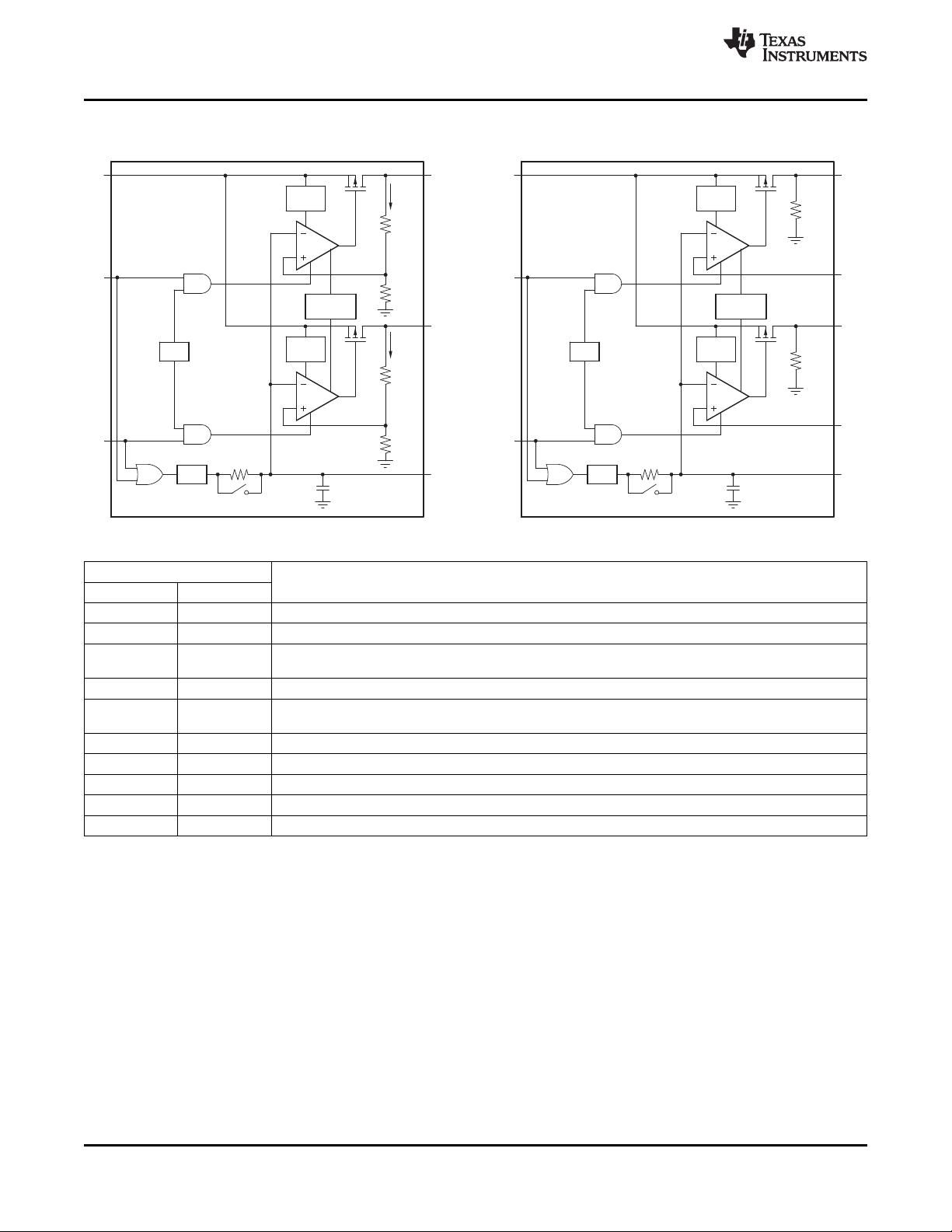
The TPS71202 low-dropout (LDO) voltage regulator
Limit
is tailored to noise-sensitive and RF applications. It
features dual 250-mA LDOs with ultra-low noise, high
• Available in Thermally-Enhanced SON
power-supply rejection ratio (PSRR), and fast
Package: 3 mm × 3 mm × 1 mm
transient and start-up response. Each regulator
output is stable with low-cost 2.2-mF ceramic output
APPLICATIONS
capacitors and features very low dropout voltages
• Cellular and Cordless Phones
(125 mV typical at 250 mA). The regulator achieves
• Wireless PDA/Handheld Products
fast start-up times (approximately 60 ms with a
0.001-mF bypass capacitor) while consuming very low
• PCMCIA/Wireless LAN Applications
quiescent current (300 mA typical with both outputs
• Digital Camera/Camcorder/Internet Audio
enabled). When the device is placed in standby
• DSP/FPGA/ASIC/Controllers and Processors
mode, the supply current is reduced to less than
0.3 mA typical. The regulator exhibits approximately
32 mVrms of output voltage noise with V
OUT
= 2.8 V
and a 0.01-mF noise reduction (NR) capacitor.
Applications with analog components that are
noise-sensitive, such as portable RF electronics,
benefit from high PSRR, low noise, and fast line and
load transient features. The TPS71202 is offered in a
thin 3-mm × 3-mm SON package and is fully
specified from –55°C to 125°C (T
J
).
(1) Custom temperature ranges available
1
Please be aware that an important notice concerning availability, standard warranty, and use in critical applications of Texas
Instruments semiconductor products and disclaimers thereto appears at the end of this data sheet.
PRODUCTION DATA information is current as of publication date.
Copyright © 2008–2010, Texas Instruments Incorporated
Products conform to specifications per the terms of the Texas
On products compliant to MIL-PRF-38535, all parameters are
Instruments standard warranty. Production processing does not
tested unless otherwise noted. On all other products, production
necessarily include testing of all parameters.
processing does not necessarily include testing of all parameters.
EN1
FB1
EN2
FB2
NR
10
9
8
7
6
IN
NC
OUT1
OUT2
GND
1
2
3
4
5
DRC PACKAGE
3-mm y 3-mm SON
(TOP VIEW)
80
70
60
50
40
30
20
10
0
PSRR (dB)
10 100 1k 10k 100k 1M 10M
Frequency (Hz)
PSRR (RIPPLE REJECTION) vs FREQUENCY
V
OUT
= 2.8 V
C
OUT
= 2.2
µ
F
C
NR
= 0.01
µ
F
I
OUT
= 1 mA
I
OUT
= 250 mA
TPS71202-EP
SGLS395A –OCTOBER 2008–REVISED SEPTEMBER 2010
www.ti.com
This integrated circuit can be damaged by ESD. Texas Instruments recommends that all integrated circuits be handled with
appropriate precautions. Failure to observe proper handling and installation procedures can cause damage.
ESD damage can range from subtle performance degradation to complete device failure. Precision integrated circuits may be more
susceptible to damage because very small parametric changes could cause the device not to meet its published specifications.
ORDERING INFORMATION
(1)
T
J
PACKAGE
(2)
ORDERABLE PART NUMBER TOP-SIDE MARKING
–55°C to 125°C SON-10 – DRC Reel of 250 TPS71202MDRCTEP CVQ
(1) For the most current package and ordering information, see the Package Option Addendum at the end of this document, or see the TI
web site at www.ti.com.
(2) Package drawings, thermal data, and symbolization are available at www.ti.com/packaging.
ABSOLUTE MAXIMUM RATINGS
over operating junction temperature range unless otherwise noted
(1)
V
IN
Input voltage range IN –0.3 V to 6 V
V
EN1
,
Input voltage range EN1, EN2 –0.3 V to V
IN
+ 0.3 V
V
EN2
V
OUT
Output voltage range OUT –0.3 V to 6 V
Peak output current Internally limited
Output short-circuit duration Indefinite
Continuous total power dissipation See Thermal Information table
T
J
Junction temperature range –55°C to 150°C
Storage temperature range –65°C to 150°C
Human-Body Model (HBM) 2000 V
ESD Electrostatic discharge rating
Charged-Device Model (CDM) 500 V
(1) Stresses beyond those listed under absolute maximum ratings may cause permanent damage to the device. These are stress ratings
only, and functional operation of the device at these or any other conditions beyond those indicated under the Electrical Characteristics
is not implied. Exposure to absolute maximum rated conditions for extended periods may affect device reliability.
2 Submit Documentation Feedback Copyright © 2008–2010, Texas Instruments Incorporated
Product Folder Link(s): TPS71202-EP
TPS71202-EP
www.ti.com
SGLS395A –OCTOBER 2008–REVISED SEPTEMBER 2010
THERMAL INFORMATION
TPS71202-EP
THERMAL METRIC
(1)(2)
UNITS
DRC (10 PINS)
q
JA
Junction-to-ambient thermal resistance 49.6
q
JCtop
Junction-to-case (top) thermal resistance 70.0
q
JB
Junction-to-board thermal resistance 17.8
°C/W
y
JT
Junction-to-top characterization parameter 0.6
y
JB
Junction-to-board characterization parameter 15.2
q
JCbot
Junction-to-case (bottom) thermal resistance 5.2
(1) For more information about traditional and new thermal metrics, see the IC Package Thermal Metrics application report, SPRA953.
(2) For thermal estimates of this device based on PCB copper area, see the TI PCB Thermal Calculator.
ELECTRICAL CHARACTERISTICS
over operating temperature range (T
J
= –55°C to +125°C), V
IN
= highest (V
OUT(nom)
+ 1 V) or 2.7 V (whichever is greater),
I
OUT
= 1 mA, V
EN1, 2
= 1.2 V, C
OUT
= 10 mF, C
NR
= 0.01 mF, and adjustable LDOs are tested at V
OUT
= 3.0 V (unless otherwise
noted). Typical values are at T
J
= 25°C.
PARAMETER TEST CONDITIONS MIN TYP MAX UNIT
V
IN
Input voltage range
(1)
2.7 5.5 V
V
FB
Internal reference (adjustable LDOs) 1.200 1.225 1.250 V
Output voltage range
V
FB
5.5 – V
DO
V
(adjustable LDOs)
Nominal T
J
= +25°C, I
OUT
= 0 mA –1.5 +1.5
V
OUT
Over V
IN
,
Accuracy
(1)
%
I
OUT
, and V
OUT
+ 1.0 V ≤ V
IN
≤ 5.5 V,
–3 1 +3
temperatur 0 mA ≤ I
OUT
≤ 250 mA
e
ΔV
OUT
%/ΔV
IN
Line regulation
(1)
V
OUT
+ 1.0 V ≤ V
IN
≤ 5.5 V 0.05 %/V
ΔV
OUT
%/ΔI
OU
Load regulation 0 mA ≤ I
OUT
≤ 250 mA 0.8 %/mA
T
Dropout voltage
V
DO
I
OUT1
= I
OUT2
= 250 mA 125 315 mV
(V
IN
= V
OUT(nom)
– 0.1V)
I
CL
Output current limit V
OUT
= 0.9 × V
OUT(nom)
400 600 800 mA
One LDO
I
OUT
= 1 mA (enabled channel) 190 250
enabled
I
GND
Ground pin current mA
Both LDOs
I
OUT1
= I
OUT2
= 1 mA to 250 mA 300 600
enabled
I
SHDN
Shutdown current
(2)
V
EN
≤ 0.4 V, 0 V ≤ V
IN
≤ 5.5 V 0.3 2.0 mA
I
FB
FB pin current 0.1 1.50 mA
No C
NR
, I
OUT
= 250 mA 80.0 × V
OUT
Output noise voltage,
V
n
mVrms
BW = 10 Hz to 100 kHz
C
NR
= 0.01 mF, I
OUT
= 250 mA 11.8 × V
OUT
f = 100 Hz, I
OUT
= 250 mA 65
Power-supply rejection ratio
PSRR dB
(ripple rejection)
f = 10 kHz, I
OUT
= 250 mA 65
t
STR
Startup time V
OUT
= 2.85 V, R
L
= 30Ω, C
NR
= 0.001 mF 60 ms
V
IH
Enable threshold high (EN1, EN2) 1.2 V
IN
V
V
IL
Enable threshold low (EN1, EN2) 0 0.4 V
I
EN
Enable pin current (EN1, EN2) V
IN
= V
EN
= 5.5 V –1 1 mA
Shutdown Temp increasing +160
T
SD
Thermal shutdown temperature °C
Reset Temp decreasing +140
Undervoltage lockout threshold V
IN
rising 2.25 2.65 V
UVLO
Undervoltage lockout hysteresis V
IN
falling 100 mV
(1) Minimum V
IN
= (V
OUT
+ V
DO
) or 2.7 V, whichever is greater.
(2) For the adjustable version, this applies only after V
IN
is applied; then V
EN
transitions from high to low.
Copyright © 2008–2010, Texas Instruments Incorporated Submit Documentation Feedback 3
Product Folder Link(s): TPS71202-EP
Current
Limit
Thermal
Shutdown
V
REF
1.225 V
UVLO
30
µ
A
EN1
OUT1IN
Current
Limit
OUT2
NR
EN2
250 k
Ω
Quickstart
5 pF
TPS712xx
Fixed/Fixed
30
µ
A
V
REF
1.225 V
UVLO
EN1
OUT1IN
OUT2
FB1
FB2
NR
EN2
250 k
Ω
Quickstart
5 pF
TPS712xx
Adj/Adj
Current
Limit
Thermal
Shutdown
Current
Limit
90 kΩ
90 kΩ
TPS71202-EP
SGLS395A –OCTOBER 2008–REVISED SEPTEMBER 2010
www.ti.com
FUNCTIONAL BLOCK DIAGRAM — FUNCTIONAL BLOCK DIAGRAM —
FIXED VERSION ADJUSTABLE VERSION
Table 1. TERMINAL FUNCTIONS
TERMINAL
DESCRIPTION
NAME DRC
IN 1 Unregulated input supply. A small 0.1-mF capacitor should be connected from IN to GND.
GND 5, Pad Ground
Output of the regulator. A small 2.2-mF ceramic capacitor is required from this pin to ground to assure
OUT1 3
stability.
OUT2 4 Same as OUT1 but for LDO2.
Driving the enable pin (EN) high turns on LDO1. Driving this pin low puts LDO1 into shutdown mode,
EN1 10
reducing operating current. The enable pin should be connected to IN if not used.
EN2 8 Same as EN1 but controls LDO2.
FB1 9 Feedback for channel 1
FB2 7 Feedback for channel 2
NR 6 Noise reduction pin; connect an external bypass capacitor to reduce LDO output noise.
NC 2 No connection.
4 Submit Documentation Feedback Copyright © 2008–2010, Texas Instruments Incorporated
Product Folder Link(s): TPS71202-EP
剩余19页未读,继续阅读
资源评论
不觉明了
- 粉丝: 3164
- 资源: 5429
上传资源 快速赚钱
- 我的内容管理 展开
- 我的资源 快来上传第一个资源
- 我的收益 登录查看自己的收益
- 我的积分 登录查看自己的积分
- 我的C币 登录后查看C币余额
- 我的收藏
- 我的下载
- 下载帮助
最新资源
- 微信小程序 - 图书管理系统源码.zip
- 微信小程序 - 图片自适应 ,富文本解析源码.zip
- 微信小程序 - 同乐居商城:购物车合算源码
- 1、根据输入的三条边值判断能组成何种三角形,并设计测试数据进行判定覆盖测试 三条边为变量a、b、c,范围为1≤边值≤10,不在范
- SQL server 练习题目8道(小白教学).zip
- Python 手写实现 iD3 决策树算法-根据信息增益公式.zip
- 411675952289057车联助手-小窗版(三星)3.5.1.apk
- 三种快速排序方法合并在一个文件中以便直接运行的Python代码示例
- 937712277954201实习5.word
- 2程序语言基础知识pdf1_1716337722703.jpeg
资源上传下载、课程学习等过程中有任何疑问或建议,欢迎提出宝贵意见哦~我们会及时处理!
点击此处反馈
安全验证
文档复制为VIP权益,开通VIP直接复制
信息提交成功