TI-UCD8220.pdf
需积分: 5 9 浏览量
2022-10-28
20:36:01
上传
评论 4
收藏 1.52MB PDF 举报

Product
Folder
Order
Now
Technical
Documents
Tools &
Software
Support &
Community
An IMPORTANT NOTICE at the end of this data sheet addresses availability, warranty, changes, use in safety-critical applications,
intellectual property matters and other important disclaimers. PRODUCTION DATA.
UCD8220
SLUS652E –MARCH 2005–REVISED APRIL 2020
UCD8220 Digitally Managed Push-Pull Analog PWM Controllers
1
1 Features
1
• For digitally managed power supplies using μCs
or the TMS320 ™ DSP family
• Voltage or peak current mode control with cycle-
by-cycle current limiting
• Clock input from digital controller to set operating
frequency and max duty cycle
• Analog PWM comparator
• 2-MHz switching frequency
• 110-V input startup circuit and thermal shutdown
(UCD8620)
• Internal programmable slope compensation
• 3.3-V, 10-mA linear regulator
• DSP/μC compatible inputs
• Dual ±4-A TrueDrive™ integrated circuit high
current drivers
• 10-ns typical rise and fall times with 2.2-nF
• 25-ns input-to-output propagation delay
• 25-ns current sense-to-output propagation delay
• Programmable current-limit threshold
• Digital output current-limit flag
• 4.5-V to 15.5-V supply voltage range
• Rated from –40°C to 105°C
2 Applications
• Digitally managed switch mode power supplies
• Push-pull, half-bridge, or full-bridge converters
• Battery chargers
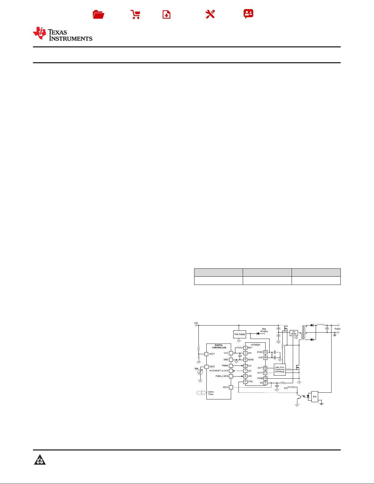
3 Description
The UCD8220 analog pulse-width modulator (PWM)
device is used in digitally managed power supplies
using a microcontroller or the TMS320 DSP family.
The UCD8220 device is a double-ended PWM
controller configured with push-pull drive logic.
Systems using the UCD8220 device close the PWM
feedback loop with traditional analog methods, but
the UCD8220 controller includes circuitry to interpret
a time-domain digital pulse train. The pulse train
contains the operating frequency and maximum duty
cycle limit which are used to control the power supply
operation. The device circuitry eases implementation
of a converter with high level control features without
the added complexity or possible PWM resolution
limitations of closing the control loop in the discrete
time domain.
The UCD8220 device can be configured for either
peak current mode or voltage mode control. The
device provides a programmable current-limit function
and a digital output current-limit flag which can be
monitored by the host controller to set the current
limit operation. For fast switching speeds, the output
stage uses the TrueDrive output circuit architecture,
which delivers rated current of ±4-A into the gate of a
MOSFET. Finally the device also includes a 3.3-V,
10-mA linear regulator to provide power to the digital
controller or act as a reference in the system.
The UCD8220 controller is compatible with the
standard 3.3-V I/O ports of UCD9K digital power
controllers, DSPs, microcontrollers, or ASICs and is
offered in the PowerPAD™ integrated circuit package
HTSSOP.
Device Information
(1)
PART NUMBER PACKAGE BODY SIZE (NOM)
UCD8220 HTSSOP (16) 5.00 mm × 4.40 mm
(1) For all available packages, see the orderable addendum at
the end of the datasheet.
Figure 1. UCD8220 Typical Simplified Push-Pull
Converter Application Schematic

剩余32页未读,继续阅读
资源评论


