没有合适的资源?快使用搜索试试~ 我知道了~
TI-TPSM5601R5HE.pdf
需积分: 9 0 下载量 144 浏览量
2022-10-25
20:32:36
上传
评论 5
收藏 1.98MB PDF 举报
温馨提示
试读
31页
TI-TPSM5601R5HE.pdf
资源详情
资源评论
资源推荐
采用增强型 Hotrod™ QFN 封装的 TPSM5601R5Hx 60V 输入、1V 至 16V 输出、
1.5A 电源模块
1 特性
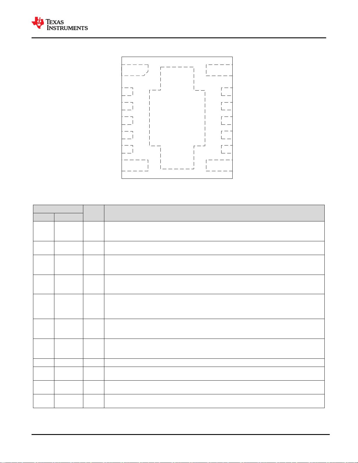
• 5mm × 5.5mm × 4mm 增强型 HotRod
™
QFN
– 出色的热性能:在 85°C 且无气流的情况下具有
高达 18W 的输出功率
– 标准封装尺寸:单个大型散热焊盘和所有引脚均
分布在封装外围
• 专为可靠耐用的应用而设计
– 宽输入电压范围:4.2V 至 60V
– 高达 66V 的输入电压瞬态保护
– 工作结温范围:–40°C 至 +125°C
– 带 EXT 后缀器件的结温范围:–55°C 至
+125°C
• 固定 1MHz 开关频率
• FPWM 运行模式
• 针对超低 EMI 要求进行了优化
– 集成屏蔽式电感器和高频旁路电容器
– 符合 EN55011 EMI 标准
– 扩频选项可降低发射
• 26µA 非开关静态电流
• 单调启动至预偏置输出
• 无环路补偿或自举组件
• 具有迟滞功能的精密使能和输入 UVLO
• 具有迟滞功能的热关断保护
• 使用 WEBENCH
®
Power Designer 创建定制稳压器
设计方案
2 应用
• 现场发送器和传感器、PLC 模块
• 恒温器、视频监控、HVAC 系统
• 交流和伺服驱动器、旋转编码器
• 工业运输、资产跟踪
• 负输出应用
3 说明
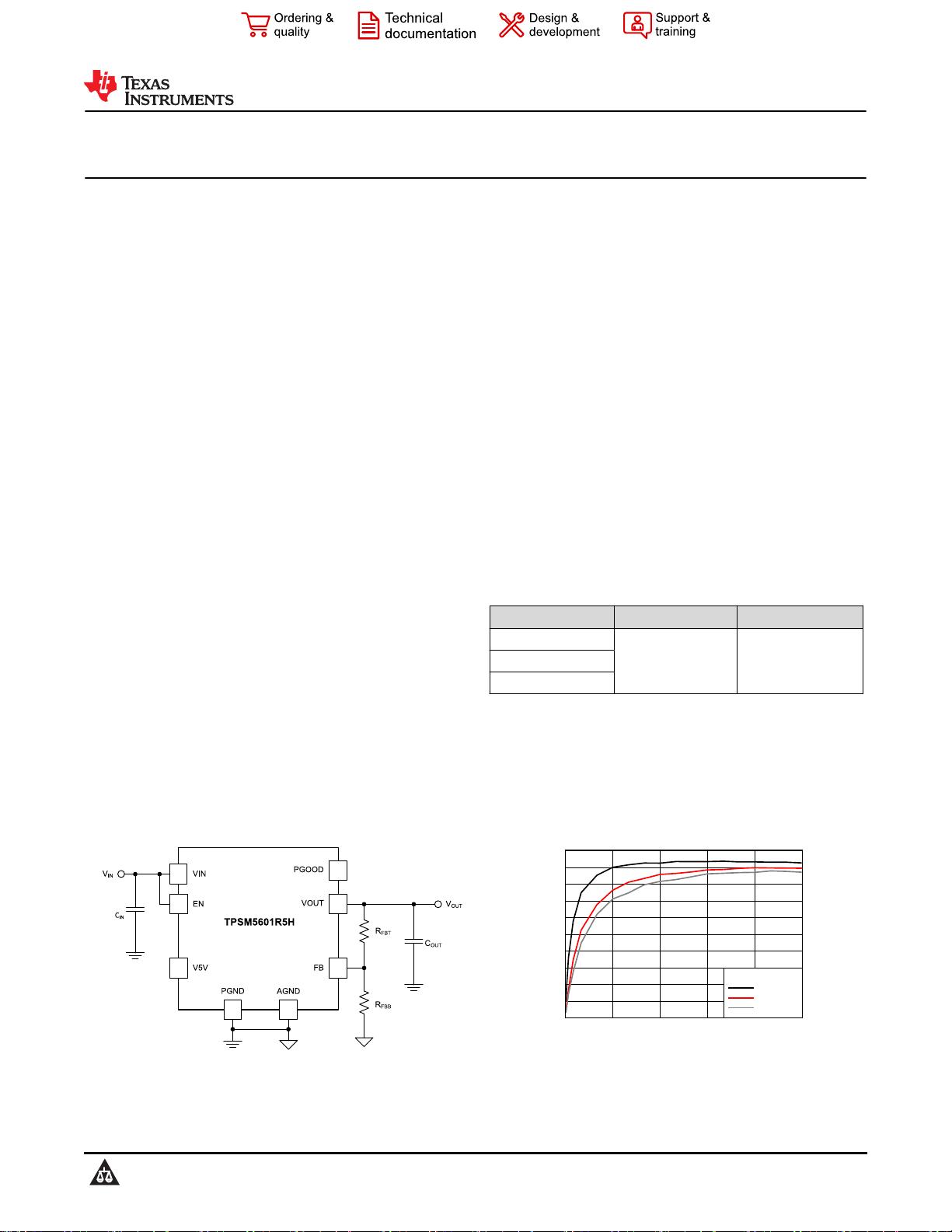
TPSM5601R5Hx 电源模块是一款高度集成的 1.5A 电
源解决方案,在热增强型 QFN 封装内整合了一个带有
功率 MOSFET 的 60V 输入降压直流/直流转换器、一
个屏蔽式电感器和多个无源器件。此 5mm × 5.5mm ×
4mm
、15 引脚 QFN 封装采用
增强型
HotRod QFN 技
术来实现增强的热性能、小尺寸和低 EMI。该封装体
的所有引脚均分布在外围,具有单个大型散热焊盘,可
在制造过程中实现简单布局和轻松处理。
TPSM5601R5Hx 是一款紧凑、易用的电源模块,具有
1.0V 至 16V 的可调节宽输出电压范围。总体解决方案
仅需四个外部组件,并且省去了设计流程中的环路补偿
和磁性元件选择。全套功能集包括电源正常状态指示、
可编程 UVLO、预偏置启动、过流和过热保护,因此
TPSM5601R5Hx 成为为各种应用供电的出色器件。空
间受限型应用可从 5mm × 5.5mm 封装中受益。此外,
TPSM5601R5HEXT 可在 –55°C 的更低温度下运行,
TPSM5601R5H
S 支持扩频运行。
器件信息
器件型号
封装
(1)
封装尺寸(标称值)
TPSM5601R5H
QFN (15) 5.0mm × 5.5mmTPSM5601R5HE
TPSM5601R5HS
(1) 如需了解所有可用封装,请参阅数据表末尾的可订购产品附
录。
半桥配置
Output Current (A)
Efficiency (%)
0 0.3 0.6 0.9 1.2 1.5
0
10
20
30
40
50
60
70
80
90
100
V
OUT
= 12 V
V
IN
= 24 V
V
IN
= 48 V
V
IN
= 60 V
典型效率 (V
OUT
= 12V)
TPSM5601R5H, TPSM5601R5HE
ZHCSMU2A – DECEMBER 2020 – REVISED MARCH 2021
本文档旨在为方便起见,提供有关 TI 产品中文版本的信息,以确认产品的概要。有关适用的官方英文版本的最新信息,请访问
www.ti.com,其内容始终优先。TI 不保证翻译的准确性和有效性。在实际设计之前,请务必参考最新版本的英文版本。
English Data Sheet: SLVSFI4
Table of Contents
1 特性................................................................................... 1
2 应用................................................................................... 1
3 说明................................................................................... 1
4 Revision History.............................................................. 2
5 Device Comparison Table...............................................2
6 Pin Configuration and Functions...................................3
7 Specifications.................................................................. 4
7.1 Absolute Maximum Ratings ....................................... 4
7.2 ESD Ratings .............................................................. 4
7.3 Recommended Operating Conditions ........................5
7.4 Thermal Information ...................................................5
7.5 Electrical Characteristics ............................................6
7.6 Typical Characteristics (VIN = 12 V)........................... 8
7.7 Typical Characteristics (VIN = 24 V)........................... 9
7.8 Typical Characteristics (VIN = 48 V)......................... 10
7.9 Typical Characteristics (VIN = 60 V)......................... 11
8 Detailed Description......................................................12
8.1 Overview................................................................... 12
8.2 Functional Block Diagram......................................... 12
8.3 Feature Description...................................................13
8.4 Device Functional Modes..........................................16
9 Applications and Implementation................................ 17
9.1 Application Information............................................. 17
9.2 Typical Application.................................................... 17
10 Power Supply Recommendations..............................19
11 Layout........................................................................... 20
11.1 Layout Guidelines................................................... 20
11.2 Layout Example...................................................... 20
12 Device and Documentation Support..........................24
12.1 Device Support....................................................... 24
12.2 Documentation Support.......................................... 24
12.3 Receiving Notification of Documentation Updates..24
12.4 支持资源..................................................................24
12.5 Trademarks............................................................. 24
12.6 静电放电警告.......................................................... 25
12.7 术语表..................................................................... 25
13 Mechanical, Packaging, and Orderable
Information.................................................................... 25
4 Revision History
Changes from Revision * (December 2020) to Revision A (March 2021) Page
• 将器件状态从“预告信息”更改为“量产数据”................................................................................................ 1
5 Device Comparison Table
DEVICE DESCRIPTION
TPSM5601R5H 60-V input voltage, 1-V to 16-V output voltage, 1.5-A power module, fixed 1-MHz switching, operating
junction temperature range: –40°C to +125°C
TPSM5601R5HS Equivalent to TPSM5601R5H, but with spread spectrum operation
TPSM5601R5HEXT
Equivalent to TPSM5601R5H, but with extended junction temperature range: –55°C to +125°C
TPSM5601R5H, TPSM5601R5HE
ZHCSMU2A – DECEMBER 2020 – REVISED MARCH 2021
www.ti.com.cn
2 Submit Document Feedback
Copyright © 2021 Texas Instruments Incorporated
Product Folder Links: TPSM5601R5H TPSM5601R5HE
6 Pin Configuration and Functions
2
3
4
5
6
13
12
11
10
9
1 14
15
7
8
VIN
EN
NC
SW
DNC
NC
VOUT VOUT
FB
AGND
V5V
PGOOD
NC
VIN
PGND
图 6-1. 15-Pin QFN RDA Package (Top View)
表 6-1. Pin Functions
PIN
TYPE
(1)
DESCRIPTION
NO. NAME
10 AGND G
Analog ground. Zero voltage reference for internal references and logic. All electrical parameters are
measured with respect to this pin. This pin must be connected to PGND at a single point. See 节 11.2
for a recommended layout.
5 DNC
—
Do not connect. Do not connect this pin to ground, to another pin, or to any other voltage. This pin is
connected to the internal bootstrap capacitor. This pin must be soldered to an isolated pad.
2 EN I
Enable pin. This pin turns the converter on when pulled high and turns off the converter when pulled low.
This pin can be connected directly to VIN. Do not float. This pin can be used to set the input
undervoltage lockout with two resistors. See 节 8.3.4.
9 FB I
Feedback input. Connect the mid-point of the feedback resistor divider to this pin. Connect the upper
resistor (R
FBT
) of the feedback divider to V
OUT
at the desired point of regulation. Connect the lower
resistor (R
FBB
) of the feedback divider to AGND.
3, 6, 13 NC
—
Not connected. These pins are not connected to any circuitry within the module. Leaving these pins
unconnected to any other signal increases spacing near the high voltage pins (VIN, SW, EN, DNC).
However, if the high voltage spacing is not needed in the application, connecting these pins to the PGND
plane can help to enhance shielding and thermal performance.
15 PGND G
Power ground. This is the return current path for the power stage of the device. Connect this pad to the
input supply return, load return, and capacitors associated with the VIN and VOUT pins. See 节 11.2 for a
recommended layout.
12 PGOOD O
Power-good pin. Open-drain output that asserts low if the feedback voltage is not within the specified
window thresholds. A 10-kΩ to 100-kΩ pullup resistor is required and can be tied to the V5V pin or other
DC voltage less than 18 V. If not used, this pin can be left open or connected to PGND.
4 SW O Switch node. Do not place any external component on this pin or connect to any signal.
1, 14 VIN I
Input supply voltage. Connect the input supply to these pins. Connect input capacitors between these
pins and PGND in close proximity to the device.
7, 8 VOUT O
Output voltage. These pins are connected to the internal output inductor. Connect these pins to the
output load and connect external output capacitors between these pins and PGND.
11 V5V O
Internal 5-V LDO output. Supplies internal control circuits. Do not connect to external loads. This pin can
be used as logic supply for PGOOD pin.
(1) G = Ground, I = Input, O = Output
www.ti.com.cn
TPSM5601R5H, TPSM5601R5HE
ZHCSMU2A – DECEMBER 2020 – REVISED MARCH 2021
Copyright © 2021 Texas Instruments Incorporated
Submit Document Feedback
3
Product Folder Links: TPSM5601R5H TPSM5601R5HE
7 Specifications
7.1 Absolute Maximum Ratings
Over the operating ambient temperature range
(1)
PARAMETER MIN MAX UNIT
Input voltage
VIN to PGND
–0.3
66
V
EN to AGND
(2)
–0.3
V
IN
+ 0.3
PGOOD to AGND
(2)
–0.3
22
FB to AGND
–0.3
5.5
AGND to PGND
–0.3
0.3
Output voltage
VOUT to PGND
(2)
–0.3
30
V
VCC to AGND 0 5.5
Operating IC junction
temperature, T
J
(3)
Non-EXT suffix device
–40
125 °C
EXT suffix device
–55
125 °C
Storage temperature, T
stg
–55
150 °C
Peak reflow case temperature 245 °C
Maximum number or reflows allowed 3
Mechanical vibration Mil-STD-883H, Method 2007.3, 1 msec, 1/2 sine, mounted 20 G
Mechanical shock Mil-STD-883H, Method 2002.5, 20 to 2000Hz 500 G
(1) Stresses beyond those listed under Absolute Maximum Ratings may cause permanent damage to the device. These are stress ratings
only, which do not imply functional operation of the device at these or any conditions beyond those indicated in Recommended
Operating Conditions. Exposure to absolute-maximum-rated conditions for extended periods may affect device reliability.
(2) The voltage on this pin must not exceed the voltage on the VIN pin by more than 0.3 V
(3) The ambient temperature is the air temperature of the surrounding environment. The junction temperature is the temperature of the
internal power IC when the device is powered. Operating below the maximum ambient temperature, as shown in the safe operating
area (SOA) curves in the typical characteristics sections, ensures that the maximum junction temperature of any component inside the
module is never exceeded.
7.2 ESD Ratings
VALUE UNIT
V
(ESD)
Electrostatic discharge
Human-body model (HBM)
(1)
±1500
V
Charged-device model (CDM)
(2)
±1500
(1) JEDEC document JEP155 states that 500-V HBM allows safe manufacturing with a standard ESD control process.
(2) JEDEC document JEP157 states that 250-V CDM allows safe manufacturing with a standard ESD control process.
TPSM5601R5H, TPSM5601R5HE
ZHCSMU2A – DECEMBER 2020 – REVISED MARCH 2021
www.ti.com.cn
4 Submit Document Feedback
Copyright © 2021 Texas Instruments Incorporated
Product Folder Links: TPSM5601R5H TPSM5601R5HE
7.3 Recommended Operating Conditions
Over operating ambient temperature range (unless otherwise noted)
(1)
MIN MAX UNIT
Input voltage, V
IN
4.2 60 V
Output voltage, V
OUT
1 16
(3)
V
Output current, I
OUT
0 1.5 A
EN voltage, V
EN
(2)
0 V
IN
V
PGOOD pullup voltage, V
PGOOD
(2)
0 18 V
Operating ambient temperature, T
A
Non-EXT suffix device
–40
105 °C
EXT suffix device
–55
105 °C
(1) Recommended operating conditions indicate conditions for which the device is intended to be functional, but do not ensure specific
performance limits. For ensured specifications, see 节 7.5.
(2) The voltage on this pin must not exceed the voltage on the VIN pin by more than 0.3 V.
(3) The recommended maximum output voltage varies depending input voltage.
7.4 Thermal Information
THERMAL METRIC
(1)
TPSM5601R5Hx
UNITRDA (QFN)
15 PINS
R
θJA
Junction-to-ambient thermal resistance
(2)
Nat Conv 20.4 °C/W
100 LFM 18.9 °C/W
200 LFM 17.6 °C/W
ψ
JT
Junction-to-top characterization parameter
(3)
3.6 °C/W
ψ
JB
Junction-to-board characterization parameter
(4)
15.3 °C/W
T
SHDN
Thermal shutdown temperature 170 °C
Recovery temperature 158 °C
(1) For more information about traditional and new thermal metrics, see the Semiconductor and IC Package Thermal Metrics app-note.
(2) The junction-to-ambient thermal resistance, R
θJA
, applies to devices soldered directly to a 6.35 cm × 8.25 cm, four-layer PCB with 2-
oz. copper. Additional airflow and PCB copper area reduces R
θJA
. See 节 11.2.1 for more information.
(3) The junction-to-top board characterization parameter, ψ
JT
, estimates the junction temperature, T
J
, of a device in a real system, using a
procedure described in JESD51-2A (section 6 and 7). T
J
= ψ
JT
× Pdis + T
T
; where Pdis is the power dissipated in the device and T
T
is
the temperature of the top of the device.
(4) The junction-to-board characterization parameter, ψ
JB
, estimates the junction temperature, T
J
, of a device in a real system, using a
procedure described in JESD51-2A (sections 6 and 7). T
J
= ψ
JB
× Pdis + T
B
; where Pdis is the power dissipated in the device and T
B
is the temperature of the board 1mm from the device.
www.ti.com.cn
TPSM5601R5H, TPSM5601R5HE
ZHCSMU2A – DECEMBER 2020 – REVISED MARCH 2021
Copyright © 2021 Texas Instruments Incorporated
Submit Document Feedback
5
Product Folder Links: TPSM5601R5H TPSM5601R5HE
剩余30页未读,继续阅读
不觉明了
- 粉丝: 3194
- 资源: 5503
上传资源 快速赚钱
- 我的内容管理 展开
- 我的资源 快来上传第一个资源
- 我的收益 登录查看自己的收益
- 我的积分 登录查看自己的积分
- 我的C币 登录后查看C币余额
- 我的收藏
- 我的下载
- 下载帮助
安全验证
文档复制为VIP权益,开通VIP直接复制
信息提交成功
评论0