

VGA Port Companion Circuit
PACVGA105
©2010 SCILLC. All rights reserved. Publication Order Number:
May 2010 Rev. 2 PACVGA105/D
Features
• Seven channels of ESD protection designed to
meet IEC-1000-4-2 Level-4 ESD requirements
(±8kV contact discharge)
• Very low loading capacitance from ESD
protection diodes at less than 5pF typical
• TTL to CMOS level-translating buffers for the
HSYNC and VSYNC lines
• Three independent supply pins (V
CC
, V
RGB
and
V
AUX
) to facilitate operation with sub-micron
Graphics Controller ICs
• High impedance pull-ups (50kΩ nominal to V
AUX
)
for HSYNC and VSYNC inputs
• Pull-up resistors (1.8kΩ nominal to V
CC
) for
DDC_CLK and DDC_DATA lines
• Compact 16-pin QSOP package
• Lead-free version available
Applications
• ESD protection and termination resistors for VGA
(video) port interfaces
• Desktop PCs
• Notebook computers
• LCD monitors
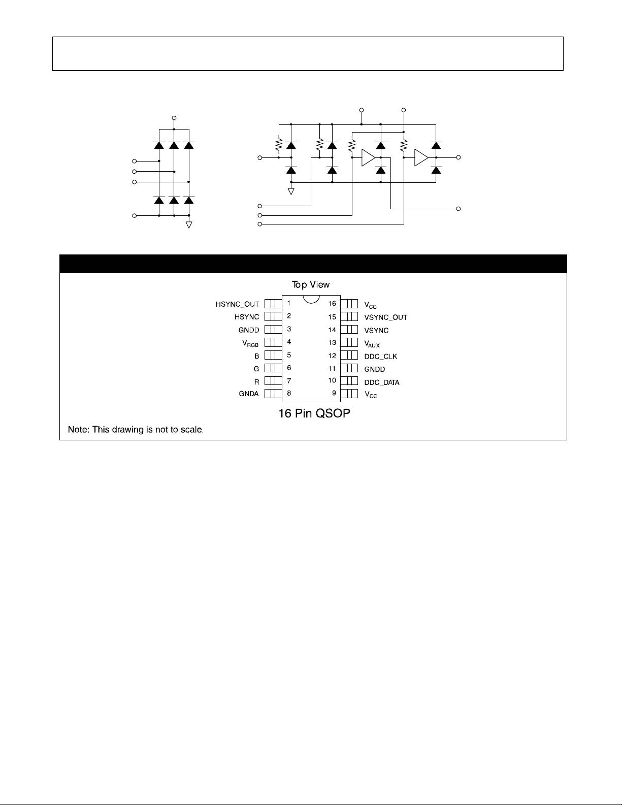
Product Description
The PACVGA105 incorporates 7 channels of ESD
protection for signal lines commonly found in a VGA
port for PCs. ESD protection is implemented with
current steering diodes designed to safely handle the
high peak surge currents associated with the IEC-
1000-4-2 Level-4 ESD Protection Standard (±8kV
contact discharge). When the channels are subjected
to an electrostatic discharge, the ESD current pulse
is diverted via the protection diodes into the positive
supply rails or ground where they may be safely
dissipated.
The upper ESD diodes for the R, G and B channels
are connected to a separate supply rail (V
RGB
) to
facilitate interfacing to graphics controller ICs with low
voltage supplies. The remaining channels are
connected to the main 5V rail (V
CC
). The lower diodes
for the R, G and B channels are also connected to a
dedicated ground pin (GNDA) to minimize crosstalk
due to common ground impedance.
Two non-inverting buffers are also included in this IC
for buffering the HSYNC and VSYNC signals from
the graphics controller IC. These buffers will accept
TTL input levels and convert them to CMOS output
levels that swing between GND and V
CC
. These
drivers have a nominal 60
Ω output impedance to
match the characteristic impedance of the HSYNC
and VSYNC lines of the video cables typically used.
The inputs of these drivers also have high impedance
pull-ups (50kW nom.) pulling up to the V
AUX
rail. In
addition, the DDC_CLOCK and DDC_DATA
channels have 1.8k
Ω resistors pulling these inputs
up to the main 5V (V
CC
) rail.
剩余8页未读,继续阅读
资源评论


weixin_38743481
- 粉丝: 698
- 资源: 4万+


最新资源
- 数据结构上机实验大作业-线性表选题.zip
- 字幕网页文字检测20-YOLO(v5至v11)、COCO、CreateML、Paligemma、TFRecord、VOC数据集合集.rar
- 雪毅云划算试客系统v2.9.7标准版 含购物返利+免费试用+9.9包邮+品牌折扣+推广中心等
- 冒泡排序算法详解及Java与Python实现
- 实时 零代码、全功能、强安全 ORM 库 后端接口和文档零代码,前端(客户端) 定制返回 JSON 的数据和结构
- 混合有源滤波器(HAPF) MATLAB-Simulink仿真 仿真模拟的HAPF补偿前后,系统所含的谐波对比如下图所示
- csi-driver-nfs
- 认识小动物-教案反思.docx
- pdfjs2.5.207和4.9.155
- 2023-04-06-项目笔记 - 第三百五十五阶段 - 4.4.2.353全局变量的作用域-353 -2025.12.22
- OPCClient-UA源码OPC客户端源码(c#开发) 另外有opcserver,opcclient的da,ua版本的见其他链接 本项目为VS2019开发,可用VS其他版本的编辑器打开项目 已应
- 2023-04-06-项目笔记 - 第三百五十五阶段 - 4.4.2.353全局变量的作用域-353 -2025.12.22
- PHP快速排序算法实现与优化
- deploy.yaml
- 家庭用具检测15-YOLO(v8至v11)数据集合集.rar
- RuoYi-Cloud-Plus 微服务通用权限管理系统
资源上传下载、课程学习等过程中有任何疑问或建议,欢迎提出宝贵意见哦~我们会及时处理!
点击此处反馈


