JEDEC
STANDARD
Package Warpage Measurement of
Surface-Mount Integrated Circuits at
Elevated Temperature
JESD22-B112B
(Revision of JESD22-B112A, October 2009)
AUGUST 2018
JEDEC SOLID STATE TECHNOLOGY ASSOCIATION

NOTICE
JEDEC standards and publications contain material that has been prepared, reviewed, and
approved through the JEDEC Board of Directors level and subsequently reviewed and approved
by the JEDEC legal counsel.
JEDEC standards and publications are designed to serve the public interest through eliminating
misunderstandings between manufacturers and purchasers, facilitating interchangeability and
improvement of products, and assisting the purchaser in selecting and obtaining with minimum
delay the proper product for use by those other than JEDEC members, whether the standard is to
be used either domestically or internationally.
JEDEC standards and publications are adopted without regard to whether or not their adoption
may involve patents or articles, materials, or processes. By such action JEDEC does not assume
any liability to any patent owner, nor does it assume any obligation whatever to parties adopting
the JEDEC standards or publications.
The information included in JEDEC standards and publications represents a sound approach to
product specification and application, principally from the solid state device manufacturer
viewpoint. Within the JEDEC organization there are procedures whereby a JEDEC standard or
publication may be further processed and ultimately become an ANSI standard.
No claims to be in conformance with this standard may be made unless all requirements stated in
the standard are met.
Inquiries, comments, and suggestions relative to the content of this JEDEC standard or
publication should be addressed to JEDEC at the address below, or call (703) 624-9230 or
www.jedec.org
Published by
©JEDEC Solid State Technology Association 2018
3103 North 10th Street
Suite 240 South
Arlington, VA 22201-2107
This document may be downloaded free of charge; however JEDEC retains the
copyright on this material. By downloading this file the individual agrees not to
charge for or resell the resulting material.
PRICE: Please refer to the current
Catalog of JEDEC Engineering Standards and Publications online at
http://www.jedec.org/Catalog/catalog.cfm
Printed in the U.S.A.
All rights reserved

JEDEC Standard No. 22-B112B
Page 1
Test Method B112B
(Revision of Test Method B112A)
Package Warpage Measurement of Surface-Mount Integrated Circuits
at Elevated Temperature
(From JEDEC Board Ballot JCB-18-22, formulated under the cognizance of the JC-14.1
Subcommittee on Reliability Test Methods for Packaged Devices.)
1 Scope
The purpose of this test method is to measure the deviation from uniform flatness of an
integrated circuit package body for the range of thermal conditions experienced during the
surface-mount soldering operation.
2 Background
When integrated circuit packages are subjected to the high-temperature solder reflow operation
associated with circuit board assembly, deformation and deviation from an ideal state of uniform
planar flatness, i.e., warpage, often results. The package warpage during board assembly can
cause the package terminals to have open or short circuit connections after the reflow soldering
operation. Certain package types, such as ball grid arrays (BGAs), have been found to be more
susceptible to component warpage. Intrinsic package warpage is largely driven by coefficient of
thermal expansion mismatch between the various packaging material constituents, but can also
be affected by absorbed moisture. Package warpage is temperature dependent, and the final
warpage state is a function of the entire temperature history or reflow profile.
JESD22-B108A measures device terminal coplanarity only at room temperature and cannot be
used to predict warpage at elevated temperatures. The worst-case warpage may be at room
temperature, maximum reflow temperature, or any temperature in-between; consequently,
package warpage must be characterized during the entire reflow soldering thermal cycle.
Critical engineering evaluations of the package and printed circuit board warpage should be
conducted in the laboratory under simulated reflow conditions. For many packages, warpage
can change with continued reflow cycles so this measurement should be made and reported for
the first reflow cycle.

JEDEC Standard No. 22-B112B
Page 2
Test Method B112B
(Revision of Test Method B112A)
3 Terms and definitions
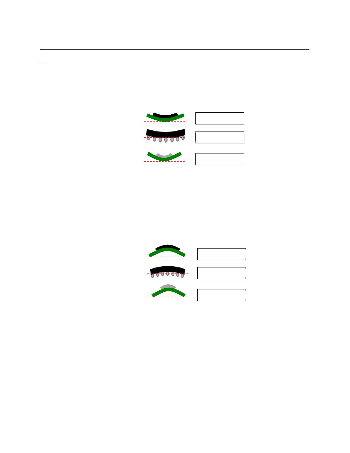
concave warpage: Negative (-) warpage resulting in the package corners being farther from
the contact plane than the center of the bottom surface of the package substrate. This is
figuratively referred as a smiling face occurrence. See Figure 1a.
Figure 1a — Package concave warpage
contact plane: A plane parallel to the reference plane passing through the lowest contact point
on the package substrate.
convex warpage: Positive (+) warpage resulting in the package corners being closer to the
contact plane than the center of the bottom surface of the package substrate. This is figuratively
referred as a frowning face occurrence. See Figure 1b.
Figure 1b — Package convex warpage
complex warpage:
Various warpage shapes that are not represented by the convex or
concave warpage such as ‘M’ shaped warpage, ‘W’ shaped warpage, or twist warpage
deviation from planarity: The difference in height between the highest point and the lowest
point on the package substrate bottom surface measured with respect to the reference plane.
digital image correlation: A 3D imaging technique utilizing multiple triangulated cameras and
computerized image matching.
fringe projection: The projection of structured light on the sample utilizing image processing to
determine package surface displacement.
Smiling (-) Concave Warpage
overmolded BGA
exposed flipchip die
Contact Plane
Contact Plane
Contact Plane
Frowning (+) Concave Warpage
overmolded BGA
exposed flipchip die
Contact Plane
Contact Plane
Contact Plane

JEDEC Standard No. 22-B112B
Page 3
Test Method B112B
(Revision of Test Method B112A)
3 Terms and definitions (cont’d)
laser reflectometry: Use of a confocal microscope to determine focal plane and thereby
measure the displacement of a surface.
package warpage: The maximum distance between the contact plane and the bottom package
surface within the measurement area.
peak reflow temperature: The maximum package reflow temperature as specified in
J-STD-020 depending on package dimensions and whether the product is intended for eutectic
Sn-Pb or Pb-free reflow soldering temperature.
rated moisture sensitivity level (MSL): The moisture sensitivity level as determined by
J-STD-020.
reference plane; regression plane: A least-squares fit of all the bottom-side or top-side
measurement points on a package.
shadow moiré: Referring to an optical noncontact method to measure warpage using a moiré
fringe pattern resulting from the geometric interference between a flat reference grating and the
projected shadow of the grating on a warped test object.
4 Reference documents (informative)
JEITA ED-7306, Measurement methods of package warpage at elevated temperature and the
maximum permissible warpage
JEP-113, Symbols and Labels for Moisture Sensitive Devices
J-STD-020, Moisture/Reflow Sensitivity Classification for Nonhermetic Solid State Surface
Mount Devices.
JESD22-A113, Preconditioning of Nonhermetic Solid State Surface Mount Components Prior to
Reliability Testing.
JESD22-B100, Physical Dimensions.
JESD22-B108, Coplanarity Test for Surface-Mount Semiconductor Devices.


