


JEDEC
STANDARD
Coplanarity Test for Surface-Mount
Semiconductor Devices
JESD22-B108B
(Revision of JESD22-B108A, January 2003)
SEPTEMBER 2010
JEDEC SOLID STATE TECHNOLOGY ASSOCIATION

NOTICE
JEDEC standards and publications contain material that has been prepared, reviewed, and
approved through the JEDEC Board of Directors level and subsequently reviewed and approved
by the JEDEC legal counsel.
JEDEC standards and publications are designed to serve the public interest through eliminating
misunderstandings between manufacturers and purchasers, facilitating interchangeability and
improvement of products, and assisting the purchaser in selecting and obtaining with minimum
delay the proper product for use by those other than JEDEC members, whether the standard is to
be used either domestically or internationally.
JEDEC standards and publications are adopted without regard to whether or not their adoption
may involve patents or articles, materials, or processes. By such action JEDEC does not assume
any liability to any patent owner, nor does it assume any obligation whatever to parties adopting
the JEDEC standards or publications.
The information included in JEDEC standards and publications represents a sound approach to
product specification and application, principally from the solid state device manufacturer
viewpoint. Within the JEDEC organization there are procedures whereby a JEDEC standard or
publication may be further processed and ultimately become an ANSI standard.
No claims to be in conformance with this standard may be made unless all requirements stated in
the standard are met.
Inquiries, comments, and suggestions relative to the content of this JEDEC standard or
publication should be addressed to JEDEC at the address below, or call (703) 907-7559 or
www.jedec.org
Published by
©JEDEC Solid State Technology Association 2010
3103 North 10th Street
Suite 240 South
Arlington, VA 22201-2107
This document may be downloaded free of charge; however JEDEC retains the
copyright on this material. By downloading this file the individual agrees not to
charge for or resell the resulting material.
PRICE: Contact JEDEC
Printed in the U.S.A.
All rights reserved

JEDEC Standard No. 22-B108B
Page 1
Test Method B108B
(Revision of B108A)
TEST METHOD B108B
COPLANARITY TEST FOR SURFACE-MOUNT SEMICONDUCTOR DEVICES
(From JEDEC Board Ballot JCB-02-122 and JCB-10-33, formulated under the cognizance of the JC-14.1
Subcommittee on Reliability Test Methods for Packaged Devices.)
1 Scope
The purpose of this test is to measure the deviation of the terminals (leads or solder balls) from
coplanarity at room temperature for surface-mount semiconductor devices. This test method is applicable
for inspection and device characterization. If package warpage or coplanarity is to be characterized at
reflow soldering temperatures, then JESD22-B112 should be used.
2 Apparatus
The equipment utilized in this test shall be capable of measuring the deviation of the terminals from
coplanarity to specified tolerances as determined by the applicable procurement document. Equipment
must be capable of measurement accuracies within +/- 10% of the specified deviation.
3 Terms and definitions
deviation from coplanarity: The distance between the intended contact point of the terminal
and the established seating plane or regression plane.
regression plane: A plane that (1) passes through the apex of the terminal that has the greatest
perpendicular distance from the package substrate, and (2) is parallel to the best-fit plane through the
apexes of all terminals determined using the method of least squares.
NOTE The regression plane may be used to emulate the package coplanarity during reflow soldering at the point
of surface mounting.
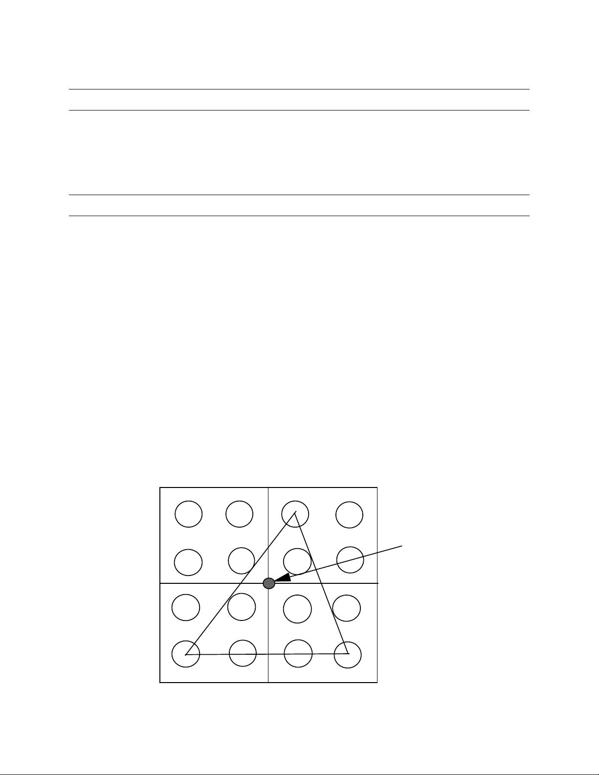
seating plane: The plane formed by the three terminal apexes that exhibit the greatest perpendicular
distance from the package substrate, provided that the triangle formed by those three apexes encompasses
the projection of the center of gravity (COG) of the component.
terminal: An externally available point of connection.
terminal apex: The point on the terminal surface that exhibits the greatest perpendicular distance from
the package substrate.
JEDEC Standard No. 22-B108B
Page 2
Test Method B108B
(Revision of B108A)
4 Reference
JEP95, Design Guide 4.17, BGA (Ball Grid Array) Package Measuring and Methodology.
JESD22-B112, Package Warpage Measurement of Surface-Mount Integrated Circuits at Elevated
Temperature.
5 Procedure
There are two methods suitable for measurement of coplanarity. They are the seating plane method and
the regression plane method. Each procedure produces a coplanarity value within the limits of error
expected for this measurement. Traditionally, the seating plane method of measuring deviation from
coplanarity is preferred. However, the regression plane method is an acceptable alternative provided the
results obtained correlate to those of the seating plane method.
5.1 Seating plane method
The following procedures are to be used:
a) Care must be taken in handling to ensure no damage to the terminals.
b) The seating plane shall be in the horizontal position with the device placed as shown in Figure 1. It is
preferable that the component terminals be measured while the component is in the dead-bug (leads-
up) position.
c) When coplanarity measurements are made, there shall be no external forces applied to the device.
d) Determine the apex of each and every terminal .
e) Determine the three terminal apexes that exhibit the greatest perpendicular distance from the
substrate. These form the seating plane, see Figure 1.
Projection
of C.O.G.
Figure 1 — Three apexes forming the seating plane and encompassing projection of C.O.G


