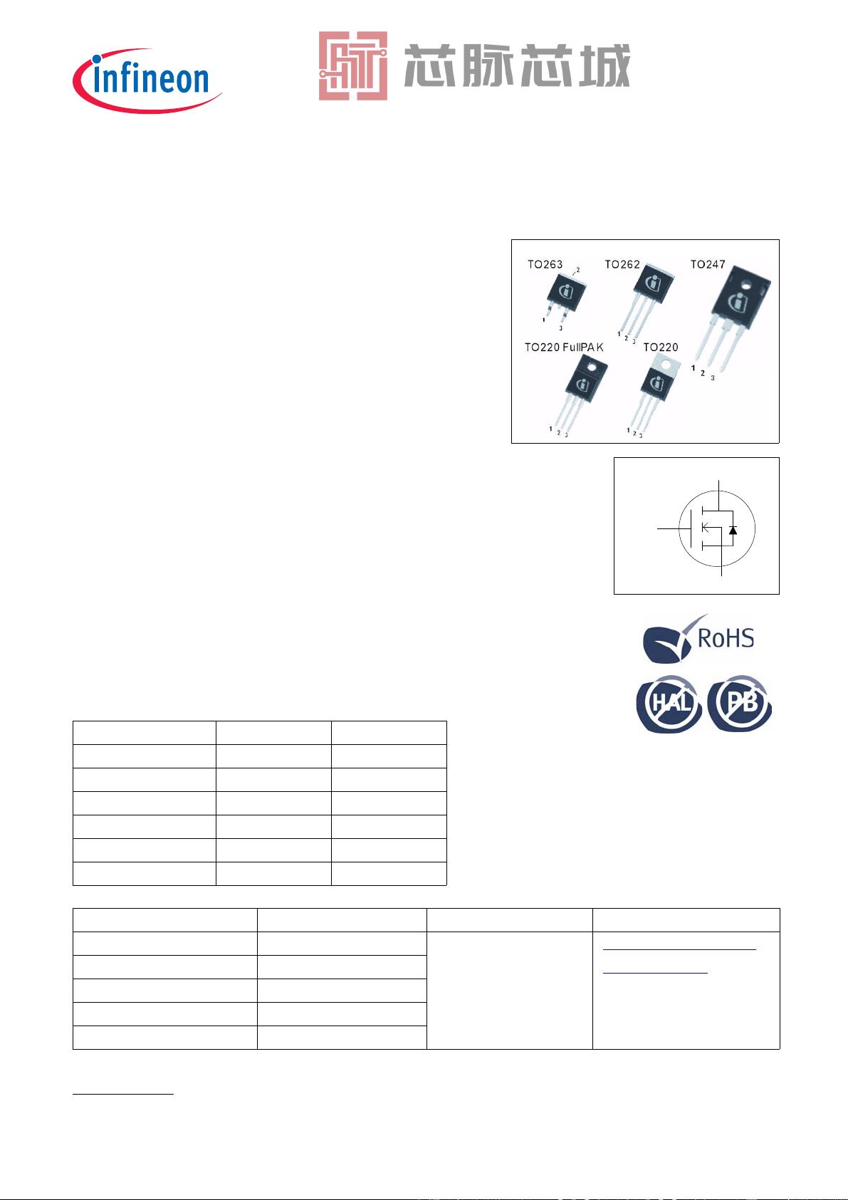
没有合适的资源?快使用搜索试试~ 我知道了~
IPI65R190C6 英飞凌芯片 INFINEON 中文版规格书手册.pdf
需积分: 5 0 下载量 117 浏览量
2023-06-29
09:59:08
上传
评论
收藏 2.36MB PDF 举报
温馨提示
试读
19页
IPI65R190C6 英飞凌芯片 INFINEON 中文版规格书手册
资源推荐
资源详情
资源评论
Industrial & Multimarket
Data Sheet
Rev. 2.0, 2011-05-09
Final
CoolMOS C6
650V CoolMOS™ C6 Power Transistor
IPx65R190C6
MOSFET
Metal Oxide Semiconductor Field Effect Transistor
drain
pin 2
gate
pin 1
source
pin 3
650V CoolMOS™ C6 Power Transistor IPA65R190C6, IPB65R190C6
IPI65R190C6, IPP65R190C6
IPW65R190C6
Final Data Sheet 2 Rev. 2.0, 2011-05-09
1 Description
CoolMOS™ is a revolutionary technology for high voltage power
MOSFETs, designed according to the superjunction (SJ) principle
and pioneered by Infineon Technologies. CoolMOS™ C6 series
combines the experience of the leading SJ MOSFET supplier with
high class innovation. The offered devices provide all benefits of a
fast switching SJ MOSFET while not sacrificing ease of use.
Extremely low switching and conduction losses make switching
applications even more efficient, more compact, lighter, and cooler.
Features
• Extremely low losses due to very low FOM R
dson*Qg and Eoss
• Very high commutation ruggedness
• Easy to use/drive
• JEDEC
1)
qualified, Pb-free plating, Halogen free
Applications
PFC stages, hard switching PWM stages and resonant switching
PWM stages for e.g. PC Silverbox, Adapter, LCD & PDP TV,
Lighting, Server, Telecom and UPS.
Please note: For MOSFET paralleling the use of ferrite beads on
the gate or separate totem poles is generally recommended.
1) J-STD20 and JESD22
Table 1 Key Performance Parameters
Parameter Value Unit
V
DS
@ T
j,max
700 V
R
DS(on),max
0.19
Q
g,typ
73 nC
I
D,pulse
66 A
E
oss
@ 400V 5.9 µJ
Body diode d
i/dt 500 A/µs
Type / Ordering Code Package Marking Related Links
IPW65R190C6 PG-TO247
IFX CoolMOS Webpage
IPB65R190C6 PG-TO263 IFX Design tools
IPI65R190C6 PG-TO262 65C6190
IPP65R190C6 PG-TO220
IPA65R190C6 PG-TO220 FullPAK
650V CoolMOS™ C6 Power Transistor
IPx65R190C6
Table of Contents
Final Data Sheet 3 Rev. 2.0, 2011-05-09
1 Description . . . . . . . . . . . . . . . . . . . . . . . . . . . . . . . . . . . . . . . . . . . . . . . . . . . . . . . . . . . . . . . . . . . . . 2
Table of Contents . . . . . . . . . . . . . . . . . . . . . . . . . . . . . . . . . . . . . . . . . . . . . . . . . . . . . . . . . . . . . . . . 3
2 Maximum ratings . . . . . . . . . . . . . . . . . . . . . . . . . . . . . . . . . . . . . . . . . . . . . . . . . . . . . . . . . . . . . . . . 4
3 Thermal characteristics . . . . . . . . . . . . . . . . . . . . . . . . . . . . . . . . . . . . . . . . . . . . . . . . . . . . . . . . . . . 5
4 Electrical characteristics . . . . . . . . . . . . . . . . . . . . . . . . . . . . . . . . . . . . . . . . . . . . . . . . . . . . . . . . . . 6
5 Electrical characteristics diagrams . . . . . . . . . . . . . . . . . . . . . . . . . . . . . . . . . . . . . . . . . . . . . . . . . 8
6 Test circuits . . . . . . . . . . . . . . . . . . . . . . . . . . . . . . . . . . . . . . . . . . . . . . . . . . . . . . . . . . . . . . . . . . . . 13
7 Package outlines . . . . . . . . . . . . . . . . . . . . . . . . . . . . . . . . . . . . . . . . . . . . . . . . . . . . . . . . . . . . . . . 14
8 Revision History . . . . . . . . . . . . . . . . . . . . . . . . . . . . . . . . . . . . . . . . . . . . . . . . . . . . . . . . . . . . . . . . 19
Table of Contents
650V CoolMOS™ C6 Power Transistor
IPx65R190C6
Maximum ratings
Final Data Sheet 4 Rev. 2.0, 2011-05-09
2 Maximum ratings
at T
j
= 25 °C, unless otherwise specified.
Table 2 Maximum ratings
Parameter Symbol Values Unit Note / Test Condition
Min. Typ. Max.
Continuous drain current
1)
1) Limited by T
j,max.
Maximum duty cycle D=0.75
I
D
--20.2 AT
C
= 25 °C
12.8 T
C
= 100°C
Pulsed drain current
2)
2) Pulse width t
p
limited by T
j,max
I
D,pulse
--66 AT
C
=25 °C
Avalanche energy, single pulse E
AS
--485 mJI
D
=3.5 A,V
DD
=50 V
Avalanche energy, repetitive E
AR
- - 0.73 I
D
=3.5 A,V
DD
=50 V
Avalanche current, repetitive I
AR
--3.5 A
MOSFET dv/dt ruggedness dv/dt - - 50 V/ns V
DS
=0...480 V
Gate source voltage V
GS
-20 - 20 V static
-30 30 AC (f>1 Hz)
Power dissipation for
TO-220, TO-247, TO-262, TO-263
P
tot
--151 WT
C
=25 °C
Power dissipation for
TO-220 FullPAK
P
tot
--34
Operating and storage temperature T
j
,T
stg
-55 - 150 °C
Mounting torque
TO-220, TO-247
- - 60 Ncm M3 and M3.5 screws
Mounting torque
TO-220 FullPAK
50 M2.5 screws
Continuous diode forward current I
S
--17.5 AT
C
=25 °C
Diode pulse current
2)
I
S,pulse
--66 AT
C
=25 °C
Reverse diode dv/dt
3)
3) Identical low side and high side switch with identical R
G
dv/dt - - 15 V/ns V
DS
=0...400 V,I
SD
I
D
,
T
j
=25 °C
Maximum diode commutation
speed
3)
di
f
/dt 500 A/µs
剩余18页未读,继续阅读
资源评论
芯脉芯城
- 粉丝: 0
- 资源: 4031
上传资源 快速赚钱
- 我的内容管理 展开
- 我的资源 快来上传第一个资源
- 我的收益 登录查看自己的收益
- 我的积分 登录查看自己的积分
- 我的C币 登录后查看C币余额
- 我的收藏
- 我的下载
- 下载帮助
安全验证
文档复制为VIP权益,开通VIP直接复制
信息提交成功