IPD80R2K0P7 英飞凌芯片 INFINEON 中文版规格书手册.pdf
需积分: 5 26 浏览量
2023-06-29
09:59:08
上传
评论
收藏 1.13MB PDF 举报

1
IPD80R2K0P7
Rev.2.1,2018-02-07Final Data Sheet
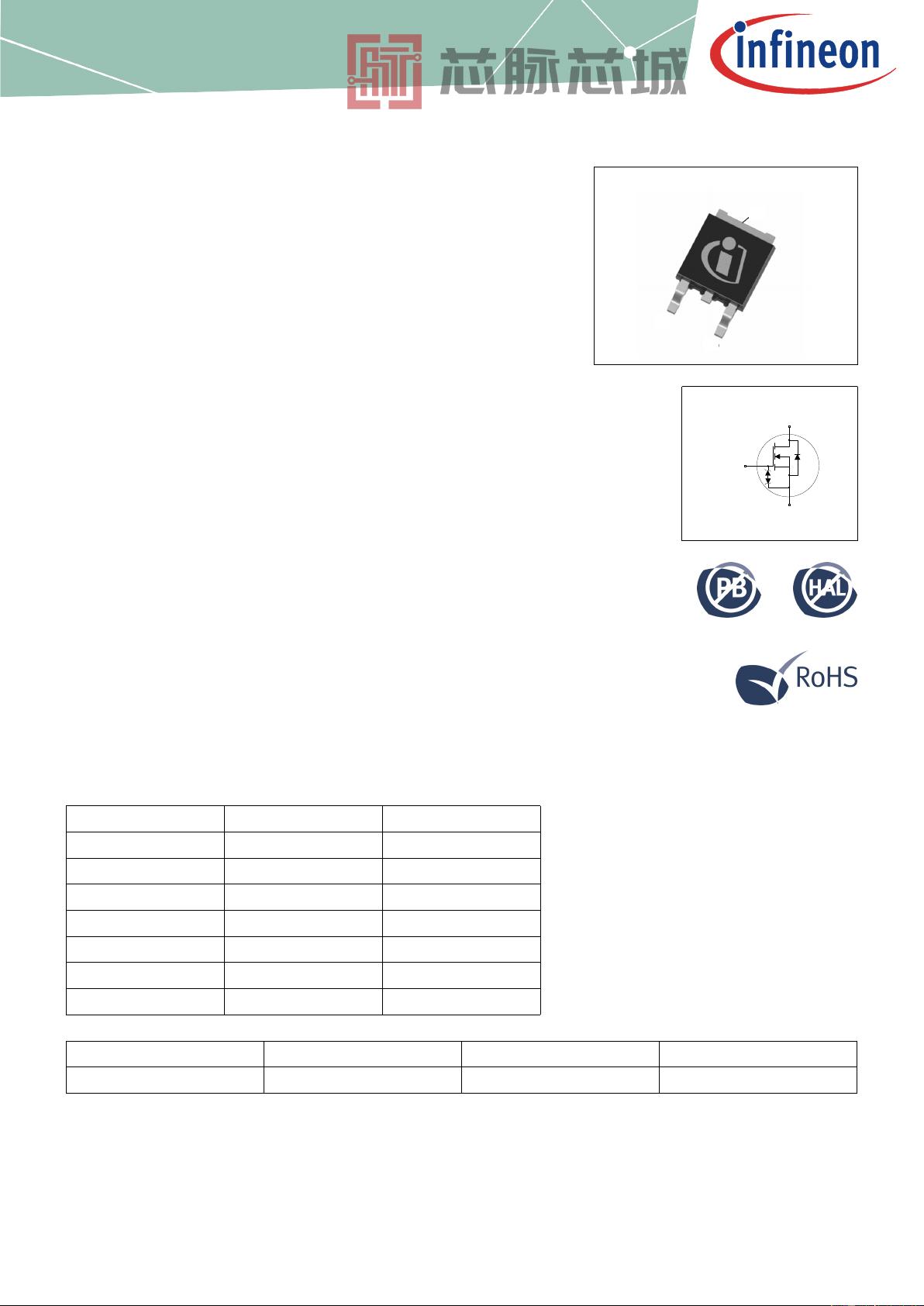
tab
1
2
3
DPAK
Drain
Pin 2, Tab
Gate
Pin 1
Source
Pin 3
MOSFET
800VCoolMOSªP7PowerTransistor
Thelatest800VCoolMOS™P7seriessetsanewbenchmarkin800V
superjunctiontechnologiesandcombinesbest-in-classperformancewith
stateoftheartease-of-use,resultingfromInfineon’sover18years
pioneeringsuperjunctiontechnologyinnovation.
Features
•Best-in-classFOMR
DS(on)
*E
oss
;reducedQ
g
,C
iss
,andC
oss
•Best-in-classDPAKR
DS(on)
•Best-in-classV
(GS)th
of3VandsmallestV
(GS)th
variationof±0.5V
•IntegratedZenerDiodeESDprotection
•Fullyqualifiedacc.JEDECforIndustrialApplications
•Fullyoptimizedportfolio
Benefits
•Best-in-classperformance
•Enablinghigherpowerdensitydesigns,BOMsavingsandlower
assemblycosts
•Easytodriveandtoparallel
•BetterproductionyieldbyreducingESDrelatedfailures
•Lessproductionissuesandreducedfieldreturns
•Easytoselectrightpartsforfinetuningofdesigns
Potentialapplications
RecommendedforhardandsoftswitchingflybacktopologiesforLED
Lighting,lowpowerChargersandAdapters,Audio,AUXpowerand
Industrialpower.AlsosuitableforPFCstageinConsumerapplications
andSolar.
Pleasenote:ForMOSFETparallelingtheuseofferritebeadsonthegate
orseperatetotempolesisgenerallyrecommended.
Table1KeyPerformanceParameters
Parameter Value Unit
V
DS
@ T
j=25°C
800 V
R
DS(on),max
2.0 Ω
Q
g,typ
9 nC
I
D
3 A
E
oss
@ 500V 0.85 µJ
V
GS(th),typ
3 V
ESD class (HBM) 1C -
Type/OrderingCode Package Marking RelatedLinks
IPD80R2K0P7 PG-TO 252-3 80R2K0P7 see Appendix A

剩余12页未读,继续阅读
资源评论


