IPD50R3K0CE 英飞凌芯片 INFINEON 中文版规格书手册.pdf
需积分: 5 32 浏览量
2023-06-28
09:21:03
上传
评论
收藏 1.54MB PDF 举报

1
IPD50R3K0CE,IPU50R3K0CE
Rev.2.3,2016-06-13Final Data Sheet
tab
1
2
3
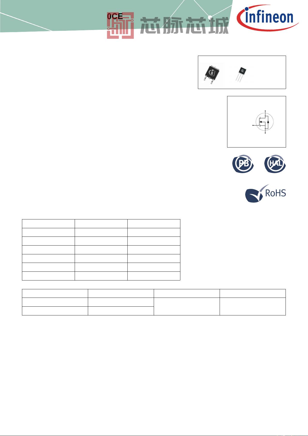
DPAK
1
2
tab
3
IPAK
Drain
Pin 2
Gate
Pin 1
Source
Pin 3
MOSFET
500VCoolMOSªCEPowerTransistor
CoolMOS™isarevolutionarytechnologyforhighvoltagepower
MOSFETs,designedaccordingtothesuperjunction(SJ)principleand
pioneeredbyInfineonTechnologies.CoolMOS™CEisa
price-performanceoptimizedplatformenablingtotargetcostsensitive
applicationsinConsumerandLightingmarketsbystillmeetinghighest
efficiencystandards.Thenewseriesprovidesallbenefitsofafast
switchingSuperjunctionMOSFETwhilenotsacrificingeaseofuseand
offeringthebestcostdownperformanceratioavailableonthemarket.
Features
•ExtremelylowlossesduetoverylowFOMRdson*QgandEoss
•Veryhighcommutationruggedness
•Easytouse/drive
•Pb-freeplating,Halogenfreemoldcompound
•Qualifiedforstandardgradeapplications
Applications
PFCstages,hardswitchingPWMstagesandresonantswitchingstages
fore.g.PCSilverbox,Adapter,LCD&PDPTVandindoorlighting.
Pleasenote:ForMOSFETparallelingtheuseofferritebeadsonthegate
orseparatetotempolesisgenerallyrecommended
Table1KeyPerformanceParameters
Parameter Value Unit
V
DS
@ T
j,max
550 V
R
DS(on),max
3 Ω
I
D
2.6 A
Q
g.typ
4.3 nC
I
D,pulse
4.1 A
E
oss
@400V 0.49 µJ
Type/OrderingCode Package Marking RelatedLinks
IPD50R3K0CE PG-TO 252
IPU50R3K0CE PG-TO 251
50S3K0CE see Appendix A


剩余13页未读,继续阅读
资源评论


