IPD200N15N3 G英飞凌芯片 INFINEON 中文版规格书手册.pdf
需积分: 5 43 浏览量
2023-06-28
09:22:26
上传
评论
收藏 1.12MB PDF 举报

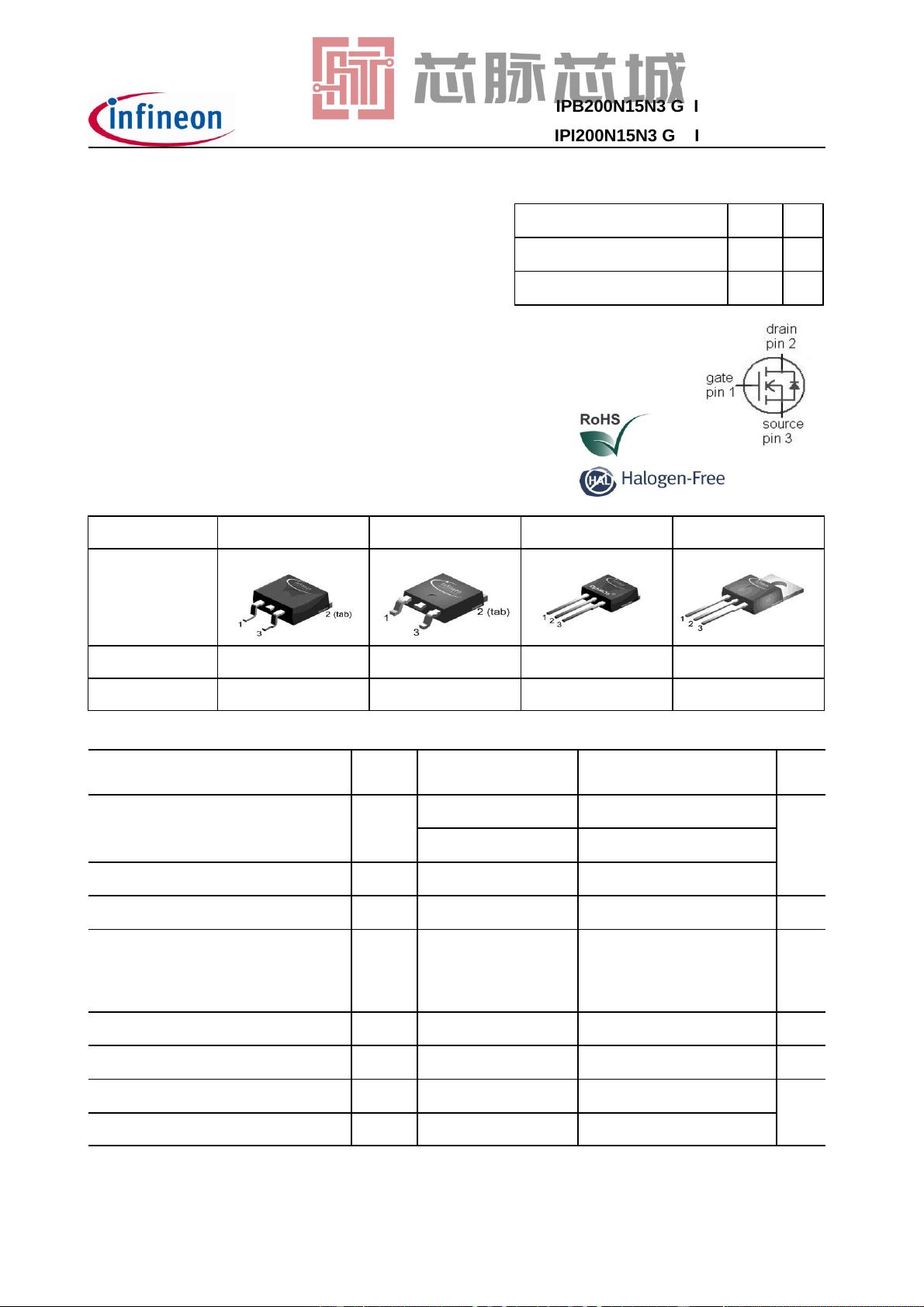
IPB200N15N3 G IPD200N15N3 G
IPI200N15N3 G IPP200N15N3 G
OptiMOS
™
3 Power-Transistor
Features
• N-channel, normal level
• Excellent gate charge x R
DS(on)
product (FOM)
• Very low on-resistance R
DS(on)
• 175 °C operating temperature
• Pb-free lead plating; RoHS compliant
• Qualified according to JEDEC
1)
for target application
• Ideal for high-frequency switching and synchronous rectification
• Halogen-free according to IEC61249-2-21
Maximum ratings, at T
j
=25 °C, unless otherwise specified
Parameter Symbol Conditions Unit
Continuous drain current
I
D
T
C
=25 °C
50 A
T
C
=100 °C
40
Pulsed drain current
2)
I
D,pulse
T
C
=25 °C
200
Avalanche energy, single pulse
E
AS
I
D
=50 A, R
GS
=25 W
170 mJ
Reverse diode dv/dt dv /dt
I
D
=50 A, V
DS
=120 V,
di/dt =100 A/µs,
T
j,max
=175 °C
6 kV/µs
Gate source voltage
V
GS
±20 V
Power dissipation
P
tot
T
C
=25 °C
150 W
Operating and storage temperature
T
j
, T
stg
-55 ... 175 °C
IEC climatic category; DIN IEC 68-1 55/175/56
Value
1)
J-STD20 and JESD22
2)
See figure 3
V
DS
150
V
R
DS(on),max
20
mW
I
D
50
A
Product Summary
Type
IPB200N15N3 G
IPD200N15N3 G
IPI200N15N3 G
IPP200N15N3 G
Package
PG-TO263-3
PG-TO252-3
PG-TO262-3
PG-TO220-3
Marking
200N15N
200N15N
200N15N
200N15N
Rev. 2.07 page 1 2014-01-09

剩余11页未读,继续阅读
资源评论


