没有合适的资源?快使用搜索试试~ 我知道了~
SPA15N60C3 英飞凌芯片 INFINEON 中文版规格书手册.pdf
需积分: 5 0 下载量 31 浏览量
2023-06-28
09:21:41
上传
评论
收藏 752KB PDF 举报
温馨提示
试读
14页
SPA15N60C3 英飞凌芯片 INFINEON 中文版规格书手册
资源推荐
资源详情
资源评论
Rev. 3.2 page 1 2009-12-22
SPP15N60C3, SPI15N60C3
SPA15N60C3
Cool MOS™
Power Transistor
V
DS
@ T
jmax
650 V
R
DS(on)
0.28 Ω
I
D
15 A
Feature
• New revolutionary high voltage technology
• Ultra low gate charge
• Periodic avalanche rated
• Extreme dv/dt rated
• Ultra low effective capacitances
• Improved transconductance
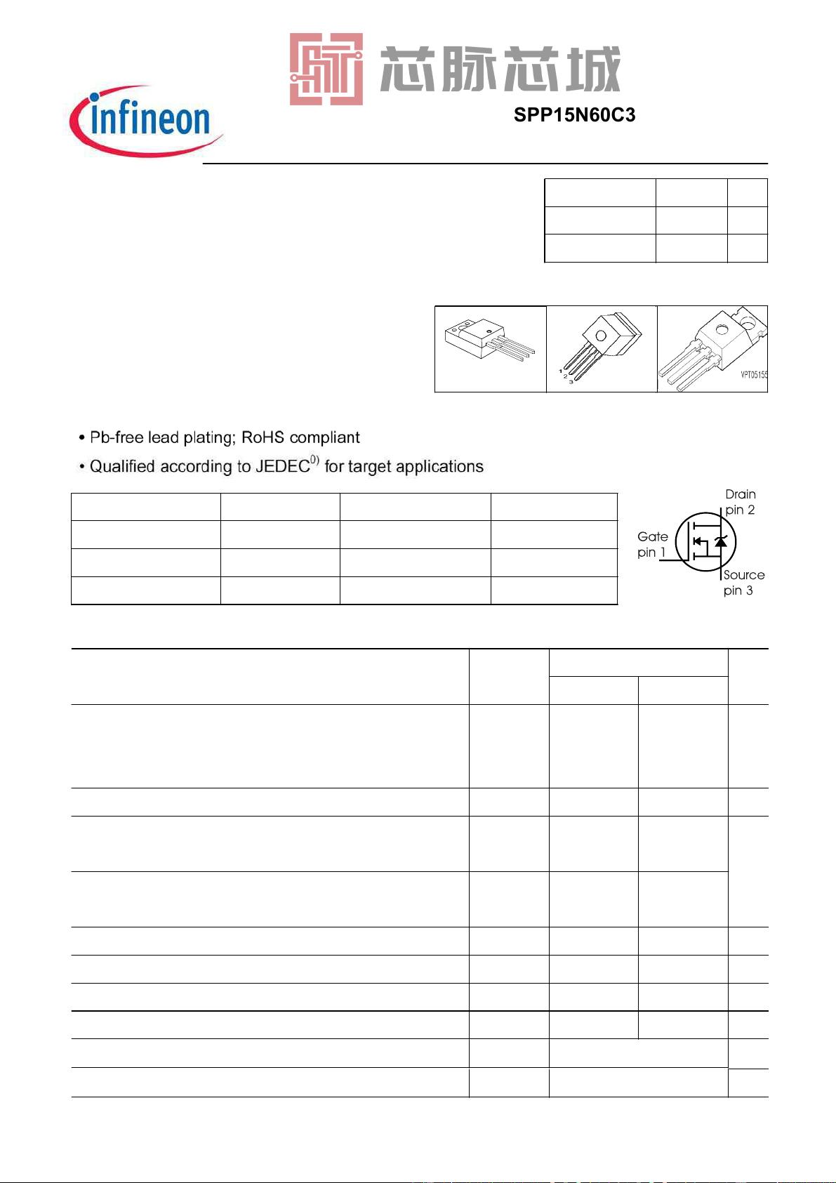
• PG-TO-220-3-31
;-3-111: Fully isolated package (2500 VAC; 1 minute)
PG-TO220FP PG-TO262 PG-TO220
P-TO220-3-31
1
2
3
Marking
15N60C3
15N60C3
15N60C3
Type Package Ordering Code
SPP15N60C3 PG-TO220 Q67040-S4600
SPI15N60C3 PG-TO262 Q67040-S4601
SPA15N60C3 PG-TO220FP SP000216325
Maximum Ratings
Parameter
Symbol Value Unit
SPA
Continuous drain current
T
C
= 25 °C
T
C
= 100 °C
I
D
15
9.4
15
1)
9.4
1)
A
Pulsed drain current, t
p
limited by T
jmax
I
D puls
45 45 A
Avalanche energy, single pulse
I
D
=7.5A, V
DD
=50V
E
AS
460 460 mJ
Avalanche energy, repetitive t
AR
limited by T
jmax
2)
I
D
=15A, V
DD
=50V
E
AR
0.8 0.8
Avalanche current, repetitive t
AR
limited by T
jmax
I
AR
15 15 A
Gate source voltage static V
GS
±20 ±20 V
Gate source voltage AC (f >1Hz)
V
GS
±30 ±30
Power dissipation, T
C
= 25°C P
tot
156 34 W
SPP_I
Operating and storage temperature
T
j
, T
stg
-55...+150 °C
Reverse diode dv/dt dv/dt 15 V/ns
6)
Rev. 3.3
Page 1
2018-02-12
SPP15N60C3, SPI15N60C3
SPA15N60C3
Maximum Ratings
Parameter
Symbol Value Unit
Drain Source voltage slope
V
DS
= 480 V, I
D
= 15 A, T
j
= 125 °C
dv/dt 50 V/ns
Thermal Characteristics
Parameter Symbol Values Unit
min. typ. max.
Thermal resistance, junction - case
R
thJC
- - 0.8 K/W
Thermal resistance, junction - case, FullPAK R
thJC
_
FP
- - 3.7
Thermal resistance, junction - ambient, leaded
R
thJA
- - 62
Thermal resistance, junction - ambient, FullPAK R
thJA
_
FP
- - 80
Soldering temperature, wavesoldering
1.6 mm (0.063 in.) from case for 10s
3)
T
sold
- - 260 °C
Electrical Characteristics, at T
j
=25°C unless otherwise specified
Parameter
Symbol Conditions Values Unit
min. typ. max.
Drain-source breakdown voltage
V
(BR)DSS
V
GS
=0V, I
D
=0.25mA 600 - - V
Drain-Source avalanche
breakdown voltage
V
(BR)DS
V
GS
=0V, I
D
=15A - 700 -
Gate threshold voltage V
GS
(
th
)
I
D
=675µA, V
GS
=V
DS
2.1 3 3.9
Zero gate voltage drain current I
DSS
V
DS
=600V, V
GS
=0V,
T
j
=25°C
T
j
=150°C
-
-
0.1
-
1
100
µA
Gate-source leakage current I
GSS
V
GS
=30V, V
DS
=0V - - 100 nA
Drain-source on-state resistance R
DS(on)
V
GS
=10V, I
D
=9.4A
T
j
=25°C
T
j
=150°C
-
-
0.25
0.68
0.28
-
Ω
Gate input resistance
R
G
f=1MHz, open drain - 1.23 -
Rev. 3.3
Page 2
2018-02-12
SPP15N60C3, SPI15N60C3
SPA15N60C3
Electrical Characteristics
Parameter
Symbol Conditions Values Unit
min. typ. max.
Transconductance g
fs
V
DS
≥2*I
D
*R
DS(on)max
,
I
D
=9.4A
- 11.9 - S
Input capacitance C
iss
V
GS
=0V, V
DS
=25V,
f=1MHz
- 1660 - pF
Output capacitance C
oss
- 540 -
Reverse transfer capacitance C
rss
- 40 -
Effective output capacitance,
4)
energy related
C
o(er)
V
GS
=0V,
V
DS
=0V to 480V
- 80 -
Effective output capacitance,
5)
time related
C
o(tr)
- 127 -
Turn-on delay time t
d(on)
V
DD
=480V, V
GS
=0/10V,
I
D
=15A,
R
G
=4.3Ω
- 10 - ns
Rise time t
r
- 5 -
Turn-off delay time t
d(off)
- 50 80
Fall time t
f
- 5 10
Gate Charge Characteristics
Gate to source charge
Q
gs
V
DD
=480V, I
D
=15A - 7 - nC
Gate to drain charge Q
gd
- 29 -
Gate charge total Q
g
V
DD
=480V, I
D
=15A,
V
GS
=0 to 10V
- 63 -
Gate plateau voltage V
(
plateau
)
V
DD
=480V, I
D
=15A - 5 - V
1
Limited only by maximum temperature
2
Repetitve avalanche causes additional power losses that can be calculated as P
AV
=E
AR
*f.
3
Soldering temperature for TO-263: 220°C, reflow
4
C
o(er)
is a fixed capacitance that gives the same stored energy as C
oss
while V
DS
is rising from 0 to 80% V
DSS
.
5
C
o(tr)
is a fixed capacitance that gives the same charging time as C
oss
while V
DS
is rising from 0 to 80% V
DSS
.
6
I
SD
<=I
D
, di/dt<=400A/us, V
DClink
=400V, V
peak
<V
BR, DSS
, T
j
<T
j,max
.
Identical low-side and high-side switch.
Rev. 3.2 page 3 2009-12-22
Rev. 3.3
Page 3
2018-02-12
剩余13页未读,继续阅读
资源评论
芯脉芯城
- 粉丝: 3
- 资源: 4031
上传资源 快速赚钱
- 我的内容管理 展开
- 我的资源 快来上传第一个资源
- 我的收益 登录查看自己的收益
- 我的积分 登录查看自己的积分
- 我的C币 登录后查看C币余额
- 我的收藏
- 我的下载
- 下载帮助
最新资源
- TG-2024-05-23-204718255.mp4
- 候志强@181 5428 8938_20240420112107.amr
- spispispispispi
- 实验二:IP协议分析.zip
- 驱动代码驱动代码驱动代码驱动代码
- SVID_20240523_141155_1.mp4
- Code for the complete guide to tkinter tutorial
- 关于百货中心供应链管理系统.zip
- SimpleFolderIcon-master 修改Unity的Project下的文件夹图标
- A python Tkinter widget to display tile based maps
资源上传下载、课程学习等过程中有任何疑问或建议,欢迎提出宝贵意见哦~我们会及时处理!
点击此处反馈
安全验证
文档复制为VIP权益,开通VIP直接复制
信息提交成功