没有合适的资源?快使用搜索试试~ 我知道了~
SPA11N60C3 英飞凌芯片 INFINEON 中文版规格书手册.pdf
需积分: 5 0 下载量 151 浏览量
2023-06-28
09:21:40
上传
评论
收藏 704KB PDF 举报
温馨提示
试读
15页
SPA11N60C3 英飞凌芯片 INFINEON 中文版规格书手册
资源推荐
资源详情
资源评论
SPP11N60C3
SPI11N60C3, SPA11N60C3, SPA11N60C3 E8185
Cool MOS™
Power Transistor
V
DS
@ T
jmax
650 V
R
DS(on)
0.38 Ω
I
D
11 A
Feature
• New revolutionary high voltage technology
• Ultra low gate charge
• Periodic avalanche rated
• Extreme dv/dt rated
• High peak current capability
• Improved transconductance
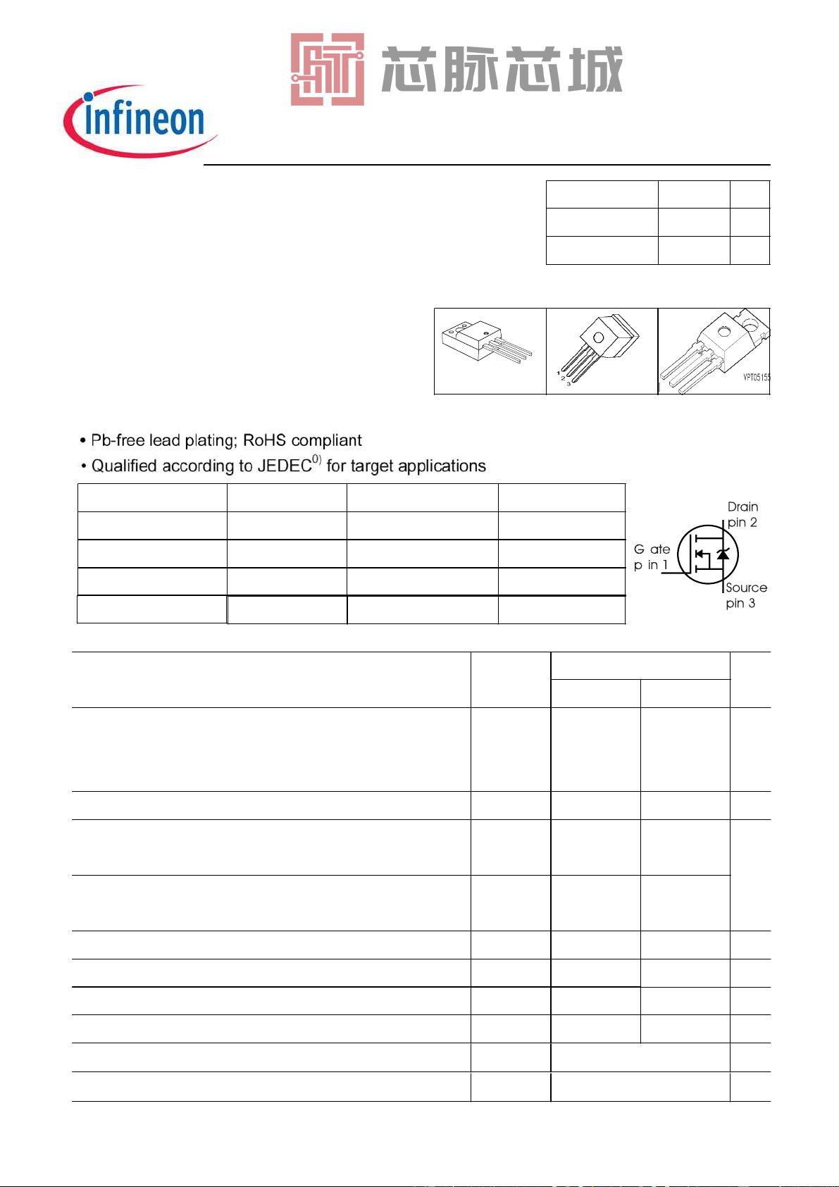
• PG-TO-220-3-31
;-3-111: Fully isolated package (2500 VAC; 1 minute)
PG-TO262PG-TO220FP PG-TO220
P-TO220-3-31
1
2
3
Marking
11N60C3
11N60C3
11N60C3
Type
Package
Ordering Code
SPP11N60C3
P
G-TO220
Q67040-S4395
SPI11N60C3
P
G-TO262
Q67042-S4403
SPA11N60C3
Q67040-S4408
Maximum Ratings
Parameter
Symbol
Value
Unit
SPA
Continuous drain current
T
C
= 25 °C
T
C
= 100 °C
I
D
11
7
11
1)
7
1)
A
Pulsed drain current,
t
p
limited by T
j
max
I
D
p
uls
33
33
A
Avalanche energy, single pulse
I
D
=5.5A, V
DD
=50V
E
AS
340
340
mJ
Avalanche energy, repetitive
t
AR
limited by T
jmax
2)
I
D
=11A, V
DD
=50V
E
AR
0.6
0.6
Avalanche current, repetitive
t
A
R
limited by T
j
max
I
AR
11
11
A
Gate source voltage static
V
GS
±20
±20
V
Gate source voltage AC (f >1Hz)
V
GS
±
30
±
30
Power dissipation,
T
C
= 25°C
P
tot
125
33
W
SPP_I
Operating and storage temperature
T
j
,
T
st
g
-55...+150
°C
Reverse diode dv/dt dv/dt 15 V/ns
7)
11N60C3
P
G-TO220
FP Q67040-S4408
SPA11N60C3E8185
11N60C3
PG-TO220
Rev. 3.3
Page 1
2018-02-09
SPP11N60C3
SPI11N60C3, SPA11N60C3, SPA11N60C3 E8185
Maximum Ratings
Parameter
Symbol Value Unit
Drain Source voltage slope
V
DS
= 480 V, I
D
= 11 A, T
j
= 125 °C
dv/dt 50 V/ns
Thermal Characteristics
Parameter
Symbol Values Unit
min. typ. max.
Thermal resistance, junction - case
R
thJC
- - 1 K/W
Thermal resistance, junction - case, FullPAK R
thJC_FP
- - 3.8
Thermal resistance, junction - ambient, leaded
R
thJA
- - 62
Thermal resistance, junction - ambient, FullPAK R
thJA_FP
- - 80
SMD version, device on PCB:
@ min. footprint
@ 6 cm
2
cooling area
3)
R
thJA
-
-
-
35
62
-
Soldering temperature, wavesoldering
1.6 mm (0.063 in.) from case for 10s
4)
T
sold
- - 260 °C
Electrical Characteristics, at T
j
=25°C unless otherwise specified
Parameter
Symbol Conditions Values Unit
min. typ. max.
Drain-source breakdown voltage
V
(BR)DSS
V
GS
=0V, I
D
=0.25mA 600 - - V
Drain-Source avalanche
breakdown voltage
V
(BR)DS
V
GS
=0V, I
D
=11A - 700 -
Gate threshold voltage V
GS(th)
I
D
=500µA, V
GS
=V
DS
2.1 3 3.9
Zero gate voltage drain current I
DSS
V
DS
=600V, V
GS
=0V,
T
j
=25°C
T
j
=150°C
-
-
0.1
-
1
100
µA
Gate-source leakage current I
GSS
V
GS
=30V, V
DS
=0V - - 100 nA
Drain-source on-state resistance R
DS(on)
V
GS
=10V, I
D
=7A
T
j
=25°C
T
j
=150°C
-
-
0.34
0.92
0.38
-
Ω
Gate input resistance
R
G
f=1MHz, open drain - 0.86 -
Rev. 3.3
Page 2
2018-02-09
SPP11N60C3
SPI11N60C3, SPA11N60C3, SPA11N60C3 E8185
Electrical Characteristics
Parameter
Symbol Conditions Values Unit
min. typ. max.
Transconductance g
fs
V
DS
≥2*I
D
*R
DS(on)max
,
I
D
=7A
- 8.3 - S
Input capacitance C
iss
V
GS
=0V, V
DS
=25V,
f=1MHz
- 1200 - pF
Output capacitance C
oss
- 390 -
Reverse transfer capacitance C
rss
- 30 -
Effective output capacitance,
5)
energy related
C
o(er)
V
GS
=0V,
V
DS
=0V to 480V
- 45 -
Effective output capacitance,
6)
time related
C
o(tr)
- 85 -
Turn-on delay time t
d(on)
V
DD
=380V, V
GS
=0/10V,
I
D
=11A,
R
G
=6.8Ω
- 10 - ns
Rise time t
r
- 5 -
Turn-off delay time t
d(off)
- 44 70
Fall time t
f
- 5 9
Gate Charge Characteristics
Gate to source charge
Q
gs
V
DD
=480V, I
D
=11A - 5.5 - nC
Gate to drain charge Q
gd
- 22 -
Gate charge total Q
g
V
DD
=480V, I
D
=11A,
V
GS
=0 to 10V
- 45 60
Gate plateau voltage V
(plateau)
V
DD
=480V, I
D
=11A - 5.5 - V
1
Limited only by maximum temperature
2
Repetitve avalanche causes additional power losses that can be calculated as P
AV
=E
AR
*f.
3
Device on 40mm*40mm*1.5mm epoxy PCB FR4 with 6cm² (one layer, 70 µm thick) copper area for drain
connection. PCB is vertical without blown air.
4
Soldering temperature for TO-263: 220°C, reflow
5
C
o(er)
is a fixed capacitance that gives the same stored energy as C
oss
while V
DS
is rising from 0 to 80% V
DSS
.
6
C
o(tr)
is a fixed capacitance that gives the same charging time as C
oss
while V
DS
is rising from 0 to 80% V
DSS
.
7
ISD<=ID, di/dt<=400A/us, VDClink=400V, Vpeak<VBR, DSS, Tj<Tj,max.
Identical low-side and high-side switch.
Rev. 3.3
Page 3
2018-02-09
剩余14页未读,继续阅读
资源评论
芯脉芯城
- 粉丝: 3
- 资源: 4031
上传资源 快速赚钱
- 我的内容管理 展开
- 我的资源 快来上传第一个资源
- 我的收益 登录查看自己的收益
- 我的积分 登录查看自己的积分
- 我的C币 登录后查看C币余额
- 我的收藏
- 我的下载
- 下载帮助
安全验证
文档复制为VIP权益,开通VIP直接复制
信息提交成功