没有合适的资源?快使用搜索试试~ 我知道了~
IRFS3207Z INFINEON 英飞凌芯片 中文版规格书手册.pdf
需积分: 5 0 下载量 121 浏览量
2023-06-25
09:57:51
上传
评论
收藏 483KB PDF 举报
温馨提示
试读
12页
IRFS3207Z INFINEON 英飞凌芯片 中文版规格书手册
资源推荐
资源详情
资源评论
Benefits
Improved Gate, Avalanche and Dynamic
dv/dt Ruggedness
Fully Characterized Capacitance and
Avalanche SOA
Enhanced body diode dV/dt and dI/dt
Capability
Lead-Free
RoHS Compliant, Halogen-Free
Applications
High Efficiency Synchronous Rectification in
SMPS
Uninterruptible Power Supply
High Speed Power Switching
Hard Switched and High Frequency Circuits
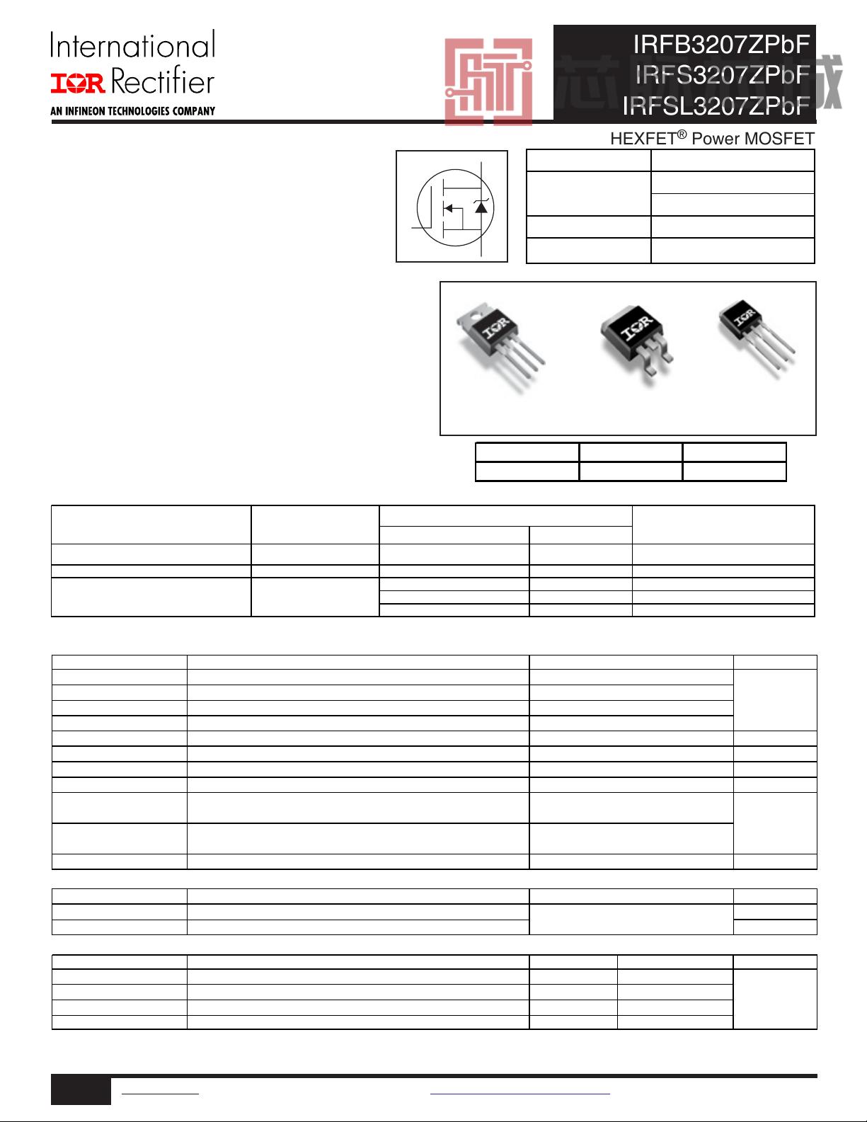
HEXFET
®
Power MOSFET
S
D
G
GDS
Gate Drain Source
TO-220AB
IRFB3207ZPbF
D
S
D
G
D
D
S
G
D
2
Pak
IRFS3207ZPbF
TO-262
IRFSL3207ZPbF
S
D
G
V
DSS
75V
R
DS
(
on
)
typ.
3.3m
Ω
max. 4.1m
Ω
I
D
(
Silicon Limited
)
170A
I
D (Package Limited)
120A
IRFB3207ZPbF
IRFS3207ZPbF
IRFSL3207ZPbF
1 www.irf.com © 2015 International Rectifier Submit Datasheet Feedback August 18, 2015
Absolute Maximum Ratings
Symbol Parameter Units
I
D
@ T
C
= 25°C Continuous Drain Current, VGS @ 10V (Silicon Limited)
I
D
@ T
C
= 100°C Continuous Drain Current, V
GS
@ 10V (Silicon Limited)
A
I
D
@ T
C
= 25°C Continuous Drain Current, V
GS
@ 10V (Wire Bond Limited)
I
DM
Pulsed Drain Current
P
D
@T
C
= 25°C Maximum Power Dissipation W
Linear Derating Factor
W/°C
V
GS
Gate-to-Source Voltage V
dv/dt
Peak Diode Recovery
V/ns
T
J
Operating Junction and °C
T
STG
Storage Temperature Range
Soldering Temperature, for 10 seconds
(1.6mm from case)
Mounting torque, 6-32 or M3 screw
Avalanche Characteristics
E
AS
(
Thermall
y
limited
)
Single Pulse Avalanche Energy
mJ
I
AR
Avalanche Current
A
E
AR
Repetitive Avalanche Energy
mJ
Thermal Resistance
Symbol Parameter Typ. Max. Units
R
θ
JC
Junction-to-Case
––– 0.50
R
θ
CS
Case-to-Sink, Flat Greased Surface , TO-220 0.50 ––– °C/W
R
θ
JA
Junction-to-Ambient, TO-220
––– 62
R
θ
JA
Junction-to-Ambient
(
PCB Mount
)
, D
2
Pak
––– 40
170
See Fig. 14, 15, 22a, 22b
300
16
-55 to + 175
± 20
2.0
10lb
in (1.1N
m)
300
Max.
170
120
670
120
Form Quantity
IRFB3207ZPbF TO-220 Tube 50 IRFB3207ZPbF
IRFSL3207ZPbF TO-262 Tube 50 IRFSL3207ZPbF
Tube 50
IRFS3207ZPbF
Tape and Reel Left 800 IRFS3207ZTRLPbF
Tape and Reel Ri
g
ht 800 IRFS3207ZTRRPbF
D2PakIRFS3207ZPbF
Base Part Number Package Type
Standard Pack
Orderable Part Number
2 www.irf.com © 2015 International Rectifier Submit Datasheet Feedback August 18, 2015
IRFB3207ZPbF/IRFS3207ZPbF/IRFSL3207ZPbF
Notes:
Calculated continuous current based on maximum allowable junction
temperature. Bond wire current limit is 120A. Note that current
limitations arising from heating of the device leads may occur with
some lead mounting arrangements.
Repetitive rating; pulse width limited by max. junction
temperature.
Limited by T
Jmax
, starting T
J
= 25°C, L = 0.033mH
R
G
= 25Ω, I
AS
= 102A, V
GS
=10V. Part not recommended for use
above this value.
S
D
G
I
SD
≤ 75A, di/dt ≤ 1730A/µs, V
DD
≤ V
(BR)DSS
, T
J
≤ 175°C.
Pulse width ≤ 400µs; duty cycle ≤ 2%.
C
oss
eff. (TR) is a fixed capacitance that gives the same charging time
as C
oss
while V
DS
is rising from 0 to 80% V
DSS
.
C
oss
eff. (ER) is a fixed capacitance that gives the same energy as
C
oss
while V
DS
is rising from 0 to 80% V
DSS
.
When mounted on 1" square PCB (FR-4 or G-10 Material). For recom
mended footprint and soldering techniques refer to application note #AN-994.
R
θ
is measured at T
J
approximately 90°C.
Static @ T
J
= 25°C (unless otherwise specified)
Symbol Parameter Min. Typ. Max. Units
V
(BR)DSS
Drain-to-Source Breakdown Voltage 75 ––– ––– V
∆V
(BR)DSS
/
∆T
J
Breakdown Voltage Temp. Coefficient ––– 0.091 ––– V/°C
R
DS(on)
Static Drain-to-Source On-Resistance ––– 3.3 4.1
mΩ
V
GS(th)
Gate Threshold Voltage 2.0 ––– 4.0 V
R
G(int)
Internal Gate Resistance
–––
0.80 ––– Ω
I
DSS
Drain-to-Source Leakage Current ––– ––– 20 µA
––– ––– 250
I
GSS
Gate-to-Source Forward Leakage ––– ––– 100 nA
Gate-to-Source Reverse Leakage ––– ––– -100
Dynamic @ T
J
= 25°C (unless otherwise specified)
Symbol Parameter Min. Typ. Max. Units
gfs Forward Transconductance 280 ––– ––– S
Q
g
Total Gate Charge ––– 120 170 nC
Q
gs
Gate-to-Source Charge ––– 27 –––
Q
gd
Gate-to-Drain ("Miller") Charge ––– 33 –––
Q
sync
Total Gate Charge Sync. (Q
g
- Q
gd
)
––– 87 –––
t
d(on)
Turn-On Delay Time ––– 20 ––– ns
t
r
Rise Time ––– 68 –––
t
d(off)
Turn-Off Delay Time ––– 55 –––
t
f
Fall Time ––– 68 –––
C
iss
Input Capacitance ––– 6920 ––– pF
C
oss
Output Capacitance ––– 600 –––
C
rss
Reverse Transfer Capacitance ––– 270 –––
C
oss
eff. (ER)
Effective Output Capacitance (Energy Related)
––– 770 –––
C
oss
eff. (TR)
Effective Output Capacitance (Time Related)
––– 960 –––
Diode Characteristics
Symbol Parameter Min. Typ. Max. Units
I
S
Continuous Source Current ––– –––
170
A
(Body Diode)
I
SM
Pulsed Source Current ––– ––– 670
(Body Diode)
V
SD
Diode Forward Voltage ––– ––– 1.3 V
t
rr
Reverse Recovery Time ––– 36 54 ns
T
J
= 25°C V
R
= 64V,
––– 41 62
T
J
= 125°C I
F
= 75A
Q
rr
Reverse Recovery Charge ––– 50 75 nC
T
J
= 25°C
di/d
t
=
100
A/
µs
––– 67 100
T
J
= 125°C
I
RRM
Reverse Recovery Current ––– 2.4 ––– A
T
J
= 25°C
t
on
Forward Turn-On Time Intrinsic turn-on time is negligible (turn-on is dominated by LS+LD)
Conditions
V
DS
= 50V, I
D
= 75A
I
D
= 75A
V
GS
= 20V
V
GS
= -20V
MOSFET symbol
showing the
V
DS
= 38V
Conditions
V
GS
= 10V
V
GS
= 0V
V
DS
= 50V
ƒ = 1.0MHz
V
GS
= 0V, V
DS
= 0V to 60V
V
GS
= 0V, V
DS
= 0V to 60V
T
J
= 25°C, I
S
= 75A, V
GS
= 0V
integral reverse
p-n junction diode.
Conditions
V
GS
= 0V, I
D
= 250µA
Reference to 25°C, I
D
= 5mA
V
GS
= 10V, I
D
= 75A
V
DS
= V
GS
, I
D
= 150µA
V
DS
= 75V, V
GS
= 0V
V
DS
= 75V, V
GS
= 0V, T
J
= 125°C
I
D
= 75A
R
G
= 2.7Ω
V
GS
= 10V
V
DD
= 49V
I
D
= 75A, V
DS
=0V, V
GS
= 10V
3 www.irf.com © 2015 International Rectifier Submit Datasheet Feedback August 18, 2015
IRFB3207ZPbF/IRFS3207ZPbF/IRFSL3207ZPbF
Fig 1. Typical Output Characteristics
Fig 3. Typical Transfer Characteristics
Fig 4. Normalized On-Resistance vs. Temperature
Fig 2. Typical Output Characteristics
Fig 6. Typical Gate Charge vs. Gate-to-Source VoltageFig 5. Typical Capacitance vs. Drain-to-Source Voltage
0.1 1 10 100
V
DS
, Drain-to-Source Voltage (V)
10
100
1000
I
D
,
D
r
a
i
n
-
t
o
-
S
o
u
r
c
e
C
u
r
r
e
n
t
(
A
)
VGS
TOP 15V
10V
8.0V
6.0V
5.5V
5.0V
4.8V
BOTTOM 4.5V
≤
60µs PULSE WIDTH
Tj = 25°C
4.5V
2 3 4 5 6 7
V
GS
, Gate-to-Source Voltage (V)
0.1
1
10
100
1000
I
D
,
D
r
a
i
n
-
t
o
-
S
o
u
r
c
e
C
u
r
r
e
n
t
(
A
)
T
J
= 25°C
T
J
= 175°C
V
DS
= 25V
≤
60µs PULSE WIDTH
-60 -40 -20 0 20 40 60 80 100120140160180
T
J
, Junction Temperature (°C)
0.5
1.0
1.5
2.0
2.5
R
D
S
(
o
n
)
,
D
r
a
i
n
-
t
o
-
S
o
u
r
c
e
O
n
R
e
s
i
s
t
a
n
c
e
(
N
o
r
m
a
l
i
z
e
d
)
I
D
= 75A
V
GS
= 10V
1 10 100
V
DS
, Drain-to-Source Voltage (V)
100
1000
10000
100000
C
,
C
a
p
a
c
i
t
a
n
c
e
(
p
F
)
V
GS
= 0V, f = 1 MHZ
C
iss
= C
gs
+ C
gd
, C
ds
SHORTED
C
rss
= C
gd
C
oss
= C
ds
+ C
gd
C
oss
C
rss
C
iss
0 20 40 60 80 100 120 140
Q
G
,
Total Gate Charge (nC)
0.0
2.0
4.0
6.0
8.0
10.0
12.0
V
G
S
,
G
a
t
e
-
t
o
-
S
o
u
r
c
e
V
o
l
t
a
g
e
(
V
)
V
DS
= 60V
V
DS
= 38V
V
DS
= 15V
I
D
= 75A
0.1 1 10 100
V
DS
, Drain-to-Source Voltage (V)
10
100
1000
I
D
,
D
r
a
i
n
-
t
o
-
S
o
u
r
c
e
C
u
r
r
e
n
t
(
A
)
4.5V
≤
60µs PULSE WIDTH
Tj = 175°C
VGS
TOP 15V
10V
8.0V
6.0V
5.5V
5.0V
4.8V
BOTTOM 4.5V
剩余11页未读,继续阅读
资源评论
芯脉芯城
- 粉丝: 3
- 资源: 4031
上传资源 快速赚钱
- 我的内容管理 展开
- 我的资源 快来上传第一个资源
- 我的收益 登录查看自己的收益
- 我的积分 登录查看自己的积分
- 我的C币 登录后查看C币余额
- 我的收藏
- 我的下载
- 下载帮助
安全验证
文档复制为VIP权益,开通VIP直接复制
信息提交成功