IRFS4127 INFINEON 英飞凌芯片 中文版规格书手册.pdf
需积分: 5 177 浏览量
2023-06-05
10:56:19
上传
评论
收藏 356KB PDF 举报

09/16/08
www.irf.com 1
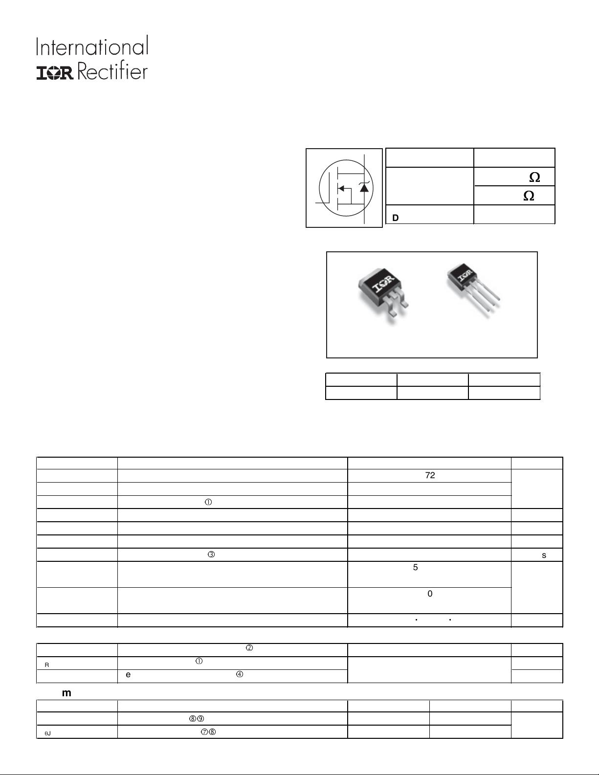
HEXFET
®
Power MOSFET
Benefits
l Improved Gate, Avalanche and Dynamic dV/dt
Ruggedness
l Fully Characterized Capacitance and Avalanche
SOA
l Enhanced body diode dV/dt and dI/dt Capability
l Lead-Free
Applications
l High Efficiency Synchronous Rectification in SMPS
l Uninterruptible Power Supply
l High Speed Power Switching
l Hard Switched and High Frequency Circuits
S
D
G
IRFS4127PbF
IRFSL4127PbF
GDS
Gate Drain Source
S
D
G
D
D
S
G
D
2
Pak
IRFS4127PbF
TO-262
IRFSL4127PbF
V
DSS
200V
R
DS(on)
typ.
18.6m
:
max.
22m
:
I
D
72A
Absolute Maximum Ratings
Symbol Parameter Units
I
D
@ T
C
= 25°C
Continuous Drain Current, V
GS
@ 10V
I
D
@ T
C
= 100°C Continuous Drain Current, V
GS
@ 10V
A
I
DM
Pulsed Drain Current
c
P
D
@T
C
= 25°C
Maximum Power Dissipation
W
Linear Derating Factor
W/°C
V
GS
Gate-to-Source Voltage
V
dv/dt
Peak Diode Recovery
e
V/ns
T
J
Operating Junction and
°C
T
STG
Storage Temperature Range
Soldering Temperature, for 10 seconds
(1.6mm from case)
Mounting torque, 6-32 or M3 screw
Avalanche Characteristics
E
AS (Thermally limited)
Sin
g
le Pulse Avalanche Ener
g
y
d
mJ
I
AR
Avalanche Current
c
A
E
AR
Repetitive Avalanche Ener
g
y
f
mJ
Thermal Resistance
Symbol Parameter Typ. Max. Units
R
θJC
Junction-to-Case
jk
–––
0.4
R
θJA
Junction-to-Ambient
ij
––– 40
Max.
72
51
300
10lb
x
in (1.1N
x
m)
300
375
57
-55 to + 175
± 20
2.5
°C/W
250
See Fig. 14, 15, 22a, 22b,
PD - 96177
资源评论


