IPW60R017C7 INFINEON 英飞凌芯片 中文版规格书手册.pdf
需积分: 5 77 浏览量
2023-06-12
10:15:29
上传
评论
收藏 1.19MB PDF 举报

1
IPW60R017C7
Rev.2.0,2016-03-01Final Data Sheet
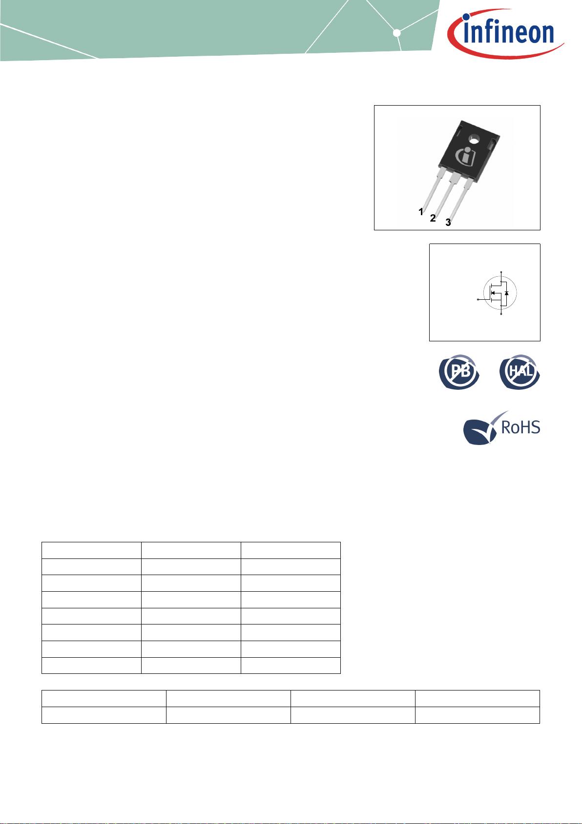
TO-247
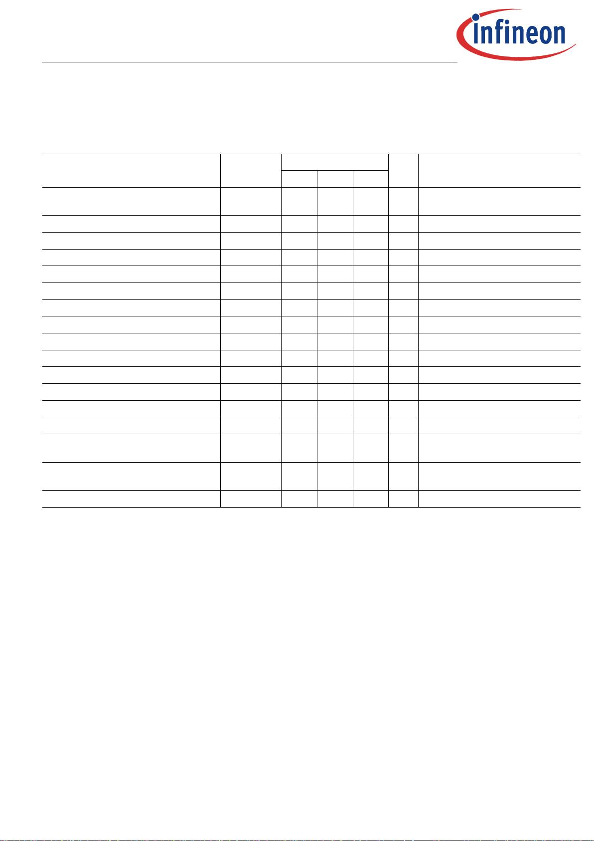
Drain
Pin 2, Tab
Gate
Pin 1
Source
Pin 3
MOSFET
600VCoolMOSªC7PowerTransistor
CoolMOS™C7isarevolutionarytechnologyforhighvoltagepower
MOSFETs,designedaccordingtothesuperjunction(SJ)principleand
pioneeredbyInfineonTechnologies.
600VCoolMOS™C7seriescombinestheexperienceoftheleadingSJ
MOSFETsupplierwithhighclassinnovation.
The600VC7isthefirsttechnologyeverwithR
DS(on)
*Abelow1Ohm*mm².
Features
•Suitableforhardandsoftswitching(PFCandhighperformanceLLC)
•IncreasedMOSFETdv/dtruggednessto120V/ns
•IncreasedefficiencyduetobestinclassFOMR
DS(on)
*E
oss
andR
DS(on)
*Q
g
•BestinclassR
DS(on)
/package
•QualifiedforindustrialgradeapplicationsaccordingtoJEDEC(J-STD20
andJESD22)
Benefits
•IncreasedeconomiesofscalebyuseinPFCandPWMtopologiesinthe
application
•Higherdv/dtlimitenablesfasterswitchingleadingtohigherefficiency
•Enablinghighersystemefficiencybylowerswitchinglosses
•Increasedpowerdensitysolutionsduetosmallerpackages
•Suitableforapplicationssuchasserver,telecomandsolar
•Higherswitchingfrequenciespossiblewithoutlossinefficiencydueto
lowEossandQg
Applications
PFCstagesandPWMstages(TTF,LLC)forhighpower/performance
SMPSe.g.Computing,Server,Telecom,UPSandSolar.
Pleasenote:ForMOSFETparallelingtheuseofferritebeadsonthegate
orseparatetotempolesisgenerallyrecommended.
Table1KeyPerformanceParameters
Parameter Value Unit
V
DS
@ T
j,max
650 V
R
DS(on),max
17 mΩ
Q
g.typ
240 nC
I
D,pulse
495 A
I
D,continuous
@ T
j
<150°C 129 A
E
oss
@400V 30 µJ
Body diode di/dt 200 A/µs
Type/OrderingCode Package Marking RelatedLinks
IPW60R017C7 PG-TO 247 60C7017 see Appendix A

剩余13页未读,继续阅读
资源评论


