没有合适的资源?快使用搜索试试~ 我知道了~
TI-DS160PR412.pdf
![preview](https://dl-preview.csdnimg.cn/87432036/0001-0eb998ace07df5349978b3cdaca205c7_thumbnail.jpeg)
![preview-icon](https://csdnimg.cn/release/downloadcmsfe/public/img/scale.ab9e0183.png)
试读
37页
![](https://csdnimg.cn/release/downloadcmsfe/public/img/starY.0159711c.png)
PCIe 4.0 线性重驱动器
PCIe 4.0 线性重驱动器(Redriver)是一种高性能的信号重驱动器,旨在支持 PCIe 4.0 和其他接口。DS160PR412 是一款四通道 PCIe 4.0 线性重驱动器,具有集成的 1:2 demultiplexer(demux),旨在解决 PCIe 4.0 通道中的信号衰减和失真问题。
特点:
* 四通道 PCIe 4.0 线性重驱动器或 repeater,具有集成的 1:2 demux
* 协议agnostic 线性重驱动器,兼容 UPI、DisplayPort、SAS、SATA、XFI 等多种协议
* 单 3.3 V 供电轨,低 120 mW/通道活动功率,无需 heat sink
* 提供高达 17 dB 的均衡增益,能够处理高达 42 dB 的 PCIe 4.0 通道衰减
* 优秀的差分返回损失(-13 dB 输入,-15 dB 输出)
* 低随机抖动(70 fs),低延迟(80 ps)
* 自动接收器检测和无缝支持 PCIe 链路训练
* 设备配置通过引脚控制或 SMBus/I2C 接口
* Mux/Demux 选择通过引脚控制
* 工业温度范围:-40°C 到 85°C
* 3.5 mm x 9 mm 42 Pin 0.5 mmPitch WQFN 封装
应用场景:
* 桌面 PC/主板
* 机架服务器
* 微服务器和塔式服务器
* 高性能计算
* 硬件加速器
* 网络附加存储
* 存储区域网络(SAN)和主机总线适配器(HBA)卡
* 网络接口卡(NIC)
工作原理:
* DS160PR412 线性重驱动器采用连续时间线性均衡器(CTLE),提供高频率 Boost
* 接收器部署 CTLE,能够打开由于intersymbol 干扰(ISI)引起的输入 eye
* 线性重驱动器与被动通道一起进行链路训练,以获得最佳的传输和接收均衡设置,从而实现最低延迟
* 低通道-通道串扰,低随机抖动和优秀的返回损失,使设备成为链路中的几乎被动元素
* 设备具有内部线性电压调节器,提供干净的电源供给高速度数据路径,提高供电噪声免疫力
DS160PR412 PCIe 4.0 线性重驱动器是 PCIe 4.0 系统中的一个关键组件,旨在解决 PCIe 4.0 通道中的信号衰减和失真问题,提高系统的可靠性和性能。
![](https://csdnimg.cn/release/download_crawler_static/87432036/bg1.jpg)
DS160PR412 PCIe® 4.0 16 Gbps 4-channel Linear Redriver with Integrated 1:2 Demux
1 Features
• Quad channel PCIe 4.0 linear redriver or repeater
with integrated 1:2 demux
• Protocol agnostic linear redriver compatible to UPI,
DisplayPort, SAS, SATA, XFI
• Single 3.3 V supply rail
• Low 120 mW /channel active power
• No heat sink required
• Provides equalization up to 17 dB at 8 GHz to
handle up to 42 dB of PCIe 4.0 channels
• Excellent differential return loss of -13 dB input and
-15 dB output
• Low additive random jitter of 70 fs with PRBS data
• Low latency of 80 ps
• Automatic receiver detection and seamless
support for PCIe link training
• Device configuration by pin control or SMBus / I
2
C.
• Mux / Demux selection through pin
• -40°C to 85°C industrial temperature range
• 3.5 mm x 9 mm 42 Pin 0.5 mm pitch WQFN
package
2 Applications
• Desktop PC/motherboard
• Rack server
• Microserver & tower server
• High performance computing
• Hardware accelerator
• Network attached storage
• Storage area network (SAN) & host bus adapter
(HBA) card
• Network interface card (NIC)
3 Description
The DS160PR412 is four channel linear redrivers with
integrated demultiplexer (demux). The low-power
high-performance linear redriver is designed to
support PCIe 4.0 and other interfaces.
The DS160PR412 receivers deploy continuous time
linear equalizers (CTLE) to provide a high-frequency
boost. The equalizer can open an input eye that is
completely closed due to inter-symbol interference
(ISI) induced by an interconnect medium, such as
PCB traces and cables. The linear redriver along with
the passive channel as a whole get link trained for
best transmit and receive equalization settings
resulting in best electrical link and lowest possible
latency. Low channel-channel cross-talk, low additive
jitter and excellent return loss allows the device to
become almost a passive element in the link. The
devices has internal linear voltage regulator to provide
clean power supply for high speed data paths that
provides high immunity to any supply noise on the
board.
The DS160PR412 implements high speed testing
during production for reliable high volume
manufacturing. The device also has low AC and DC
gain variation providing consistent equalization in high
volume platform deployment.
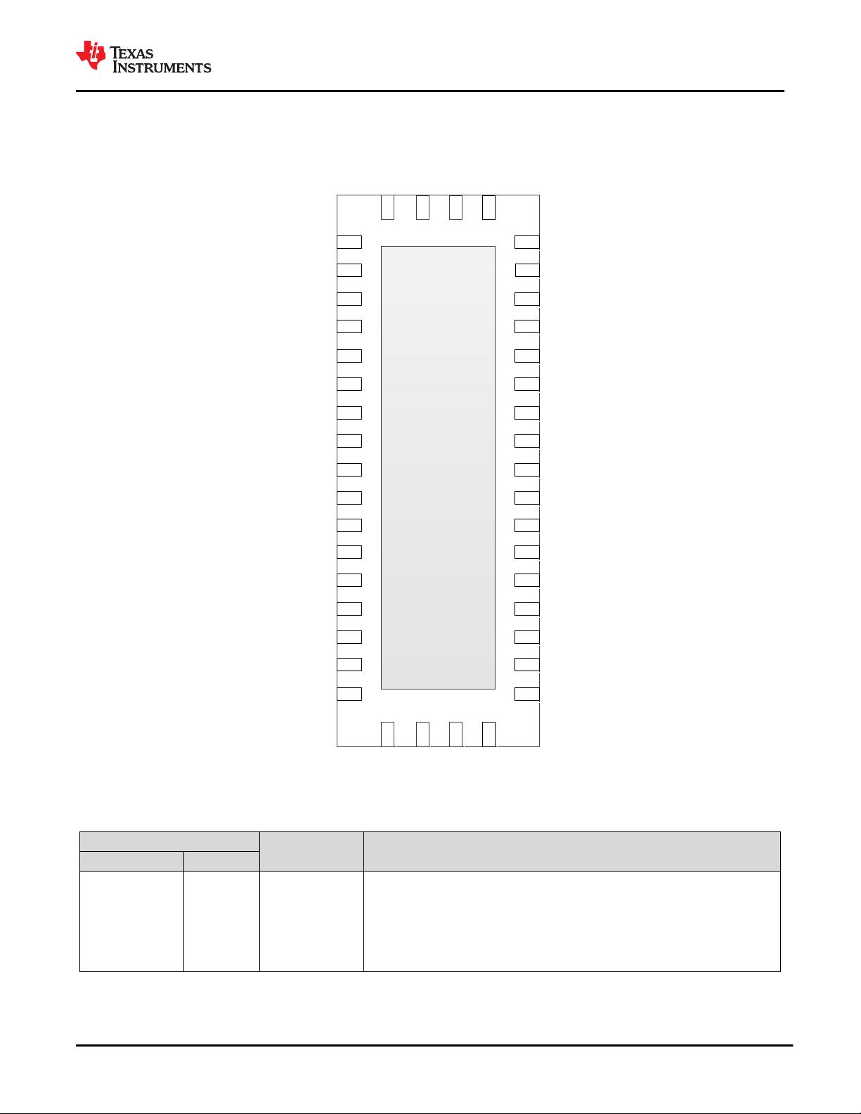
Device Information
(1)
PART NUMBER PACKAGE BODY SIZE (NOM)
DS160PR412 WQFN (42) 3.5 mm x 9 mm
(1) For all available packages, see the orderable addendum at
the end of the data sheet.
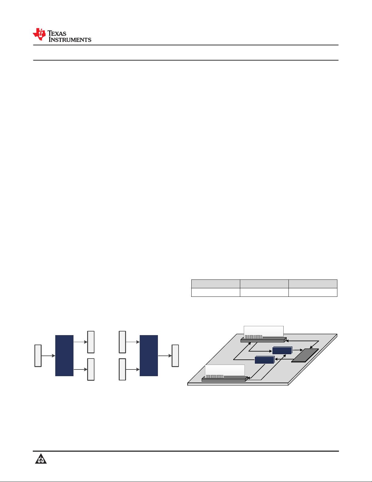
Connector-B
CPU
Connector-A
x8
Slot
x8
x16
Slot
x8
TXA 8-ch
PCIe Card
PCIe Card
TXB 8-ch
RXB 8-ch
RXA 8-ch
RX 8-ch
TX 8-ch
x8
DS160PR412
4 Ch 1:2 De-mux
DS160PR421
4 Ch 2:1 Mux
PCIe Lane MuxingDe-multiplexer
DS160PR412
Redriver Demux
RX 1RX 2
TX
4-Ch
4-Ch
4-Ch
Multiplexer
DS160PR421
Redriver Mux
RX
TX 1
4-Ch
4-Ch
TX 2
4-Ch
Application Use Case
www.ti.com
DS160PR412
SNLS685 – DECEMBER 2020
Copyright © 2020 Texas Instruments Incorporated
Submit Document Feedback
1
Product Folder Links: DS160PR412
DS160PR412
SNLS685 – DECEMBER 2020
An IMPORTANT NOTICE at the end of this data sheet addresses availability, warranty, changes, use in safety-critical applications,
intellectual property matters and other important disclaimers. PRODUCTION DATA.
![](https://csdnimg.cn/release/download_crawler_static/87432036/bg2.jpg)
Table of Contents
1 Features............................................................................1
2 Applications..................................................................... 1
3 Description.......................................................................1
4 Revision History.............................................................. 2
5 Pin Configuration and Functions...................................3
6 Specifications.................................................................. 6
6.1 Absolute Maximum Ratings ....................................... 6
6.2 ESD Ratings .............................................................. 6
6.3 Recommended Operating Conditions ........................6
6.4 Thermal Information ...................................................7
6.5 DC Electrical Characteristics ..................................... 7
6.6 High Speed Electrical Characteristics ........................8
6.7 SMBUS/I2C Timing Charateristics .............................9
6.8 Typical Characteristics.............................................. 11
7 Detailed Description......................................................14
7.1 Overview................................................................... 14
7.2 Functional Block Diagram......................................... 14
7.3 Feature Description...................................................14
7.4 Device Functional Modes..........................................16
7.5 Programming............................................................ 16
8 Application and Implementation.................................. 18
8.1 Application Information............................................. 18
8.2 Typical Applications.................................................. 18
9 Power Supply Recommendations................................23
10 Layout...........................................................................24
10.1 Layout Guidelines................................................... 24
11 Layout Example........................................................... 25
12 Device and Documentation Support..........................27
12.1 Receiving Notification of Documentation Updates..27
12.2 Support Resources................................................. 27
12.3 Trademarks.............................................................27
12.4 Electrostatic Discharge Caution..............................27
12.5 Glossary..................................................................27
13 Mechanical, Packaging, and Orderable
Information.................................................................... 28
4 Revision History
NOTE: Page numbers for previous revisions may differ from page numbers in the current version.
DATE REVISION NOTES
December 2020 * Advance Info.
DS160PR412
SNLS685 – DECEMBER 2020
www.ti.com
2 Submit Document Feedback
Copyright © 2020 Texas Instruments Incorporated
Product Folder Links: DS160PR412
![](https://csdnimg.cn/release/download_crawler_static/87432036/bg3.jpg)
5 Pin Configuration and Functions
1
1
2
2
3
3
4
4
5
5
6
6
7
7
8
8
9
9
10
10
11
11
12
12
13
13
14
14
15
15
16
16
17
17
42
42
41
41
40
40
39
39
18
18
19
19
20
20
21
21
38
38
37
37
36
36
35
35
34
34
33
33
32
32
31
31
30
30
29
29
28
28
27
27
26
26
25
25
24
24
23
23
22
22
RX_DET/SCL
MODE
GAIN/SDA
RSVD
PD
EQ0/ADDR
SEL
RX0P
RX0N
GND
RX1P
RX1N
VCC
GND
RX2P
RX2N
VCC
RX3P
RX3N
GND
VREG1
VREG2
TXA0P
GND
TXA0N
GND GND
EQ1
TXB0P
TXB0N
TXA1P
TXA1N
TXB1P
TXB1N
TXA2P
TXA2N
TXB2P
TXB2N
TXA3P
TXA3N
TXB3P
TXB3N
EP=GND
Figure 5-1. RUA Package 42-Pin WQFN Top View
Table 5-1. Pin Functions
PIN
I/O DESCRIPTION
NAME NO.
MODE 41 I, 4-level
Sets device control configuration modes. 4-level IO pin as defined in Table 7-3.
The pin can be exercised at device power up or in normal operation mode.
L0: Pin Mode – device control configuration is done solely by strap pins.
L1 or L2: SMBus/I
2
C Slave Mode – device control configuration is done by an
external controller with SMBus/I
2
C master. This pin along with ADDR pin sets
devices slave address.
L3 (Float): RESERVED – TI internal test mode.
www.ti.com
DS160PR412
SNLS685 – DECEMBER 2020
Copyright © 2020 Texas Instruments Incorporated
Submit Document Feedback
3
Product Folder Links: DS160PR412
![](https://csdnimg.cn/release/download_crawler_static/87432036/bg4.jpg)
Table 5-1. Pin Functions (continued)
PIN
I/O DESCRIPTION
NAME NO.
EQ0 /ADDR 40 I, 4-level In Pin Mode:
The EQ0 and EQ1 pins sets receiver linear equalization CTLE (AC gain) for all
channels according to Table 7-1. These pins are sampled at device power-up only.
In SMBus/I
2
C Mode:
The ADDR pin in conjunction with MODE pin sets SMBus / I
2
C slave address
according to Table 7-4. The pin is sampled at device power-up only.
EQ1 20 I, 4-level
GAIN /SDA 1 I, 4-level / IO
In Pin Mode:
DC gain (broadbad gain including high frequency) from the input to the output of
the device for all channels. Note the device also provides AC (high frequency)
gain in the form of equalization controlled by EQ pins or SMBus/I
2
C registers.
In SMBus/I
2
C Mode:
3.3 V SMBus/I
2
C data. External pullup resistor such as 4.7 kΩ required for
operation.
GND EP, 6, 9, 16,
21, 30, 39
P Ground reference for the device.
EP: the Exposed Pad at the bottom of the QFN package. It is used as the GND
return for the device. The EP should be connected to ground plane(s) through low
resistance path. A via array provides a low impedance path to GND. The EP also
improves thermal dissipation.
RSVD 19 O TI internal test pin. Keep no connect.
PD 18 I, 3.3-V LVCMOS 2-level logic controlling the operating state of the redriver. Active in both Pin Mode
and SMBus/I
2
C Mode. The pin is used part of PCIe RX_DET state machine as
outlined in Table 7-2.
High: Power down for all channels
Low: Power up, normal operation for all channels
RX_DET /SCL 42 I, 4-level / IO In Pin Mode:
Sets receiver detect state machine options according to Table 7-2. The pin is
sampled at device power-up only.
In SMBus/I
2
C Mode:
3.3 V SMBus/I
2
C clock. External pullup resistor such as 4.7 kΩ required for
operation.
RX0N 4 I Inverting differential RX inputs. Channel 0.
RX0P 3 I Noninverting differential RX inputs. Channel 0.
RX1N 8 I Inverting differential RX inputs. Channel 1.
RX1P 7 I Noninverting differential RX inputs. Channel 0.
RX2N 11 I Inverting differential RX inputs. Channel 2.
RX2P 10 I Noninverting differential RX inputs. Channel 2.
RX3N 15 I Inverting differential RX inputs. Channel 3.
RX3P 14 I Noninverting differential RX inputs. Channel 3.
SEL 17 I, 3.3 V LVCMOS Selects the mux path. Active in both Pin Mode and SMBus/I
2
C Mode. Note the
SEL pin must be exercised in system implementations for mux selection between
Port A vs Port B. The pin is used part of PCIe RX_DET state machine as outlined
in Table 7-2.
L: Port A selected.
H: Port B selected.
TXA0N 37 O Inverting differential TX output – Port A, Channel 0.
TXA0P 38 O Non-inverting differential TX output – Port A, Channel 0.
TXA1N 33 O Inverting differential TX output – Port A, Channel 1.
TXA1P 34 O Non-inverting differential TX output – Port A, Channel 1.
TXA2N 28 O Inverting differential TX output – Port A, Channel 2.
TXA2P 29 O Non-inverting differential TX output – Port A, Channel 2.
TXA3N 24 O Inverting differential TX output – Port A, Channel 3.
TXA3P 25 O Non-inverting differential TX output – Port A, Channel 3.
TXB0N 35 O Inverting differential TX output – Port B, Channel 0.
DS160PR412
SNLS685 – DECEMBER 2020
www.ti.com
4 Submit Document Feedback
Copyright © 2020 Texas Instruments Incorporated
Product Folder Links: DS160PR412
![](https://csdnimg.cn/release/download_crawler_static/87432036/bg5.jpg)
Table 5-1. Pin Functions (continued)
PIN
I/O DESCRIPTION
NAME NO.
TXB0P 36 O Non-inverting differential TX output – Port B, Channel 0.
TXB1N 31 O Inverting differential TX output – Port B, Channel 1.
TXB1P 32 O Non-inverting differential TX output – Port B, Channel 1.
TXB2N 26 O Inverting differential TX output – Port B, Channel 2.
TXB2P 27 O Non-inverting differential TX output – Port B, Channel 2.
TXB3N 22 O Inverting differential TX output – Port B, Channel 3.
TXB3P 23 O Non-inverting differential TX output – Port B, Channel 3.
VCC 5, 13 P Power supply, VCC = 3.3 V ± 10%. The VCC pins on this device should be
connected through a low-resistance path to the board VCC plane.
VREG1 2 P Internal regulator output. Must add decoupling capacitor of 0.22 µF near the pin.
Do not route the pin beyond the decoupling capacitor. Do not connect to VREG2.
Do not use as a power supply for any other component on the board.
VREG2 12 P Internal regulator output. Must add decoupling caps of 0.22 µF near the pin. Do
not route the pin beyond the decoupling capacitor. Do not connect to VREG1. Do
not use as a power supply for any other component on the board.
www.ti.com
DS160PR412
SNLS685 – DECEMBER 2020
Copyright © 2020 Texas Instruments Incorporated
Submit Document Feedback
5
Product Folder Links: DS160PR412
剩余36页未读,继续阅读
资源推荐
资源评论
![](https://csdnimg.cn/release/downloadcmsfe/public/img/starY.0159711c.png)
130 浏览量
2025-02-08 上传
2025-02-05 上传
![](https://csdnimg.cn/release/downloadcmsfe/public/img/starY.0159711c.png)
资源评论
![avatar-default](https://csdnimg.cn/release/downloadcmsfe/public/img/lazyLogo2.1882d7f4.png)
- qq_335607272023-02-14#完美解决问题 #运行顺畅 #内容详尽 #全网独家 #注释完整
- m0_745259962023-02-14#完美解决问题 #运行顺畅 #内容详尽 #全网独家 #注释完整
- CSDN_1872023-02-14#完美解决问题 #运行顺畅 #内容详尽 #全网独家 #注释完整
- 2301_763960562023-02-14#完美解决问题 #运行顺畅 #内容详尽 #全网独家 #注释完整
![avatar](https://profile-avatar.csdnimg.cn/107303f5121d47e49d12d0a9ae68af10_weixin_54787054.jpg!1)
不觉明了
- 粉丝: 8263
- 资源: 5764
上传资源 快速赚钱
我的内容管理 展开
我的资源 快来上传第一个资源
我的收益
登录查看自己的收益我的积分 登录查看自己的积分
我的C币 登录后查看C币余额
我的收藏
我的下载
下载帮助
![voice](https://csdnimg.cn/release/downloadcmsfe/public/img/voice.245cc511.png)
![center-task](https://csdnimg.cn/release/downloadcmsfe/public/img/center-task.c2eda91a.png)
最新资源
- 自媒体studio one 的插件dll 文件,不会安装的,自己看博客
- 强化学习-Birds-Code
- VW80332-2021中文版
- GPS 标准定位服务 (SPS) 性能标准
- 强化学习 -迷宫Code
- CBAM注意力机制详解
- 清华大学DeepSeek如何赋能职场应用?从提示词技巧到多场景应用
- PCAA模块加持YOLOv11-目标检测16个点暴力涨点攻略.pdf
- Mamba-YOLOv11骨干替换-阿里云最新架构优化方案解析.pdf
- LSKA大核注意力机制-YOLOv11检测头优化全流程详解.pdf
- YOLOv11+5G网络-港口集装箱自动识别与物流调度系统搭建.pdf
- YOLOv11+3D点云-物流仓储场景下的包裹体积测量与分拣系统.pdf
- YOLOv11+BEVformer-三维目标检测在自动驾驶中的融合实践.pdf
- YOLOv11+FPGA硬件加速-高速公路卡口车牌识别延迟优化指南.pdf
- YOLOv11+ROS机器人-实时动态场景下的目标抓取与避障算法详解.pdf
- YOLOv11+BEVformer实现自动驾驶多视角目标融合检测.pdf
安全验证
文档复制为VIP权益,开通VIP直接复制
![dialog-icon](https://csdnimg.cn/release/downloadcmsfe/public/img/green-success.6a4acb44.png)