TI-P82B96.pdf
需积分: 0 108 浏览量
2023-02-07
23:26:32
上传
评论 5
收藏 1.55MB PDF 举报

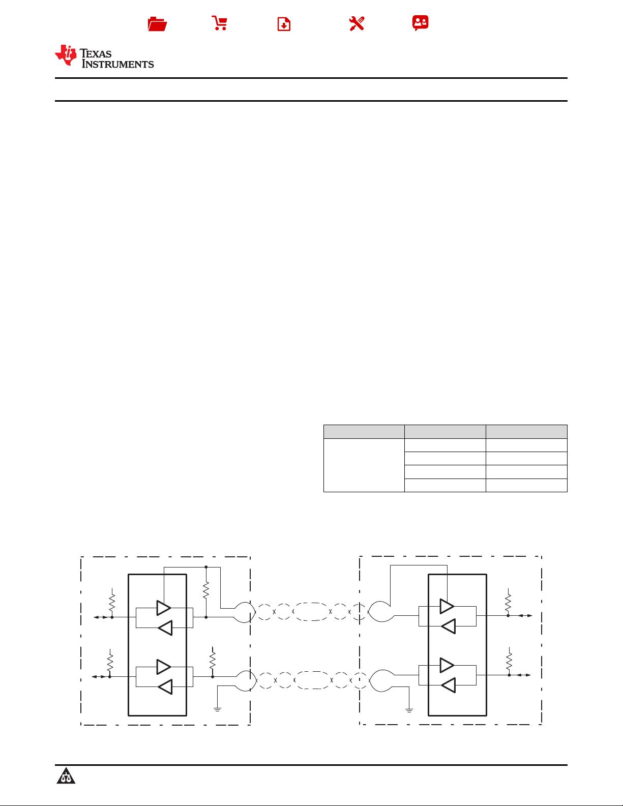
SCL
SCL
SDA
P82B96
Main Enclosure Remote-Control Enclosure
3.3–5 V
3.3–5 V
12 V
12 V
12 V
Long Cables
3.3–5 V
3.3–5 V
SDA
P82B96
Product
Folder
Sample &
Buy
Technical
Documents
Tools &
Software
Support &
Community
P82B96
SCPS144C –MAY 2006–REVISED MAY 2015
P82B96 I
2
C Compatible Dual Bidirectional Bus Buffer
1 Features 3 Description
The P82B96 device is a bus buffer that supports
1
• Operating Power-Supply Voltage Range
bidirectional data transfer between an I
2
C bus and a
of 2 V to 15 V
range of other bus configurations with different
• Can Interface Between I
2
C Buses Operating at
voltage and current levels.
Different Logic Levels (2 V to 15 V)
One of the advantages of the P82B96 is that it
• Longer Cables by allowing bus capacitance of
supports longer cables/traces and allows for more
400 pF on Main Side (Sx/Sy) and 4000 pF on
devices per I
2
C bus because it can isolate bus
Transmission Side (Tx/Ty)
capacitance such that the total loading (devices and
• Outputs on the Transmission Side (Tx/Ty) Have
trace lengths) of the new bus or remote I
2
C nodes
are not apparent to other I
2
C buses (or nodes). The
High Current Sink Capability for Driving Low-
restrictions on the number of I
2
C devices in a system
Impedance or High-Capacitive Buses
due to capacitance, or the physical separation
• Interface With Optoelectrical Isolators and Similar
between them, are greatly improved.
Devices That Need Unidirectional Input and
The device is able to provide galvanic isolation
Output Signal Paths by Splitting I
2
C Bus Signals
(optocoupling) or use balanced transmission lines
Into Pairs of Forward (Tx/Ty) and Reverse (Rx/Ry)
(twisted pairs), because separate directional Tx and
Signals
Rx signals are provided. The Tx and Rx signals may
• 400-kHz Fast I
2
C Bus Operation Over at Least
be connected directly (without causing bus latching),
20 Meters of Wire
to provide an bidirectional signal line with I
2
C
• Latch-Up Performance Exceeds 100 mA Per
properties (open-drain driver). Likewise, the Ty and
Ry signals may also be connected together to provide
JESD 78, Class II
an bidirectional signal line with I
2
C properties (open-
• ESD Protection Exceeds JESD 22
drain driver). This allows for a simple communication
design, saving design time and costs.
2 Applications
• HDMI DDC
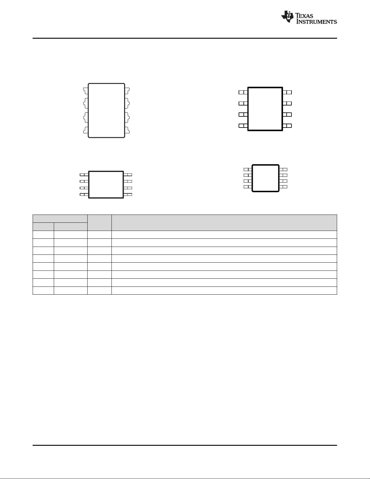
Device Information
(1)
PART NUMBER PACKAGE BODY SIZE (NOM)
• Long I
2
C Communication
SOIC (8) 4.90 mm × 3.91 mm
• Galvanic I
2
C Isolation
VSSOP (8) 3.00 mm × 3.00 mm
• Industrial Communications
P82B96
PDIP (8) 9.81 mm × 6.35 mm
TSSOP (8) 3.00 mm × 4.40 mm
(1) For all available packages, see the orderable addendum at
the end of the data sheet.
Long-Distance I
2
C Communications
1
An IMPORTANT NOTICE at the end of this data sheet addresses availability, warranty, changes, use in safety-critical applications,
intellectual property matters and other important disclaimers. PRODUCTION DATA.


剩余35页未读,继续阅读
资源评论


