TI-TCA9801.pdf
需积分: 9 147 浏览量
2023-02-07
23:23:58
上传
评论 4
收藏 1.49MB PDF 举报

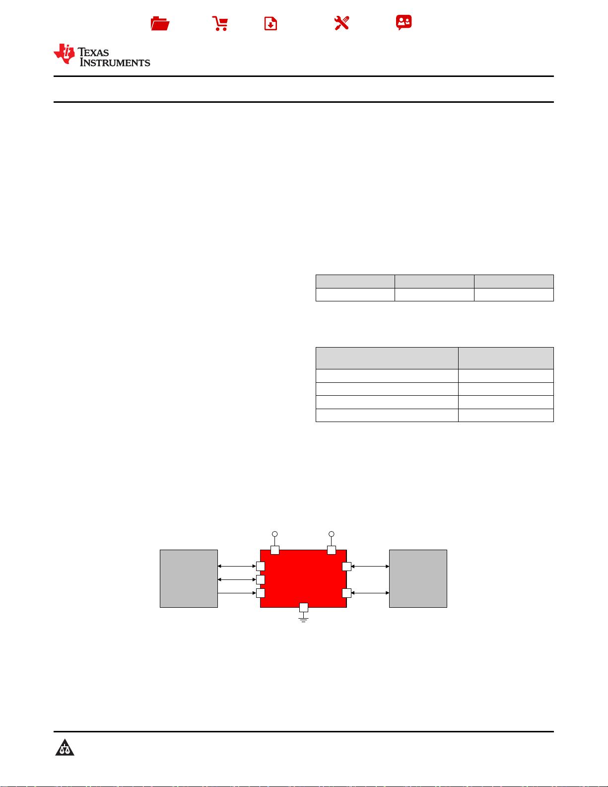
TCA9801
GND
4
1
VCCA
3 SDAA
2 SCLA
7SCLB
6SDAB
I
2
C or SMBus Master
(e.g. Processor)
5 EN
8
VCCB
I
2
C Slave Devices
Copyright © 2017, Texas Instruments Incorporated
Product
Folder
Order
Now
Technical
Documents
Tools &
Software
Support &
Community
本文档旨在为方便起见,提供有关 TI 产品中文版本的信息,以确认产品的概要。 有关适用的官方英文版本的最新信息,请访问 www.ti.com,其内容始终优先。 TI 不保证翻译的准确
性和有效性。 在实际设计之前,请务必参考最新版本的英文版本。
English Data Sheet: SCPS265
TCA9801
ZHCSG40B –MARCH 2017–REVISED FEBRUARY 2020
TCA9801 电电平平转转换换 I
2
C 总总线线缓缓冲冲器器/中中继继器器
1
1 特特性性
1
• 双通道双向缓冲器
• 在 B 侧集成了电流源,不需要外部 B 侧电阻器
• 超低功耗
• 无静态电压偏移,低 V
OL
• 与 I
2
C 总线和 SMBus 兼容
• 在 A 侧上,工作电源电压范围为 0.8V 至 3.6V
• 在 B 侧上,工作电源电压范围为 1.65V 至 3.6V
• 高电平有效中继器使能输入
• A 侧断电高阻抗 I
2
C 总线引脚
• 断电反射功率保护 I
2
C 总线引脚
• 支持时钟拉伸和多主仲裁
• 0.5mA 至 3mA 的电流源选项系列
2 应应用用
• 服务器
• 路由器(路由设备)
• 工业设备
• 个人计算机
• 功耗敏感型 应用
3 说说明明
TCA9801 是一款适用于 I
2
C 总线和 SMBus/PMBus 系
统的双通道双向缓冲器。它在低电压(低至 0.8V)和
较高电压(1.65V 至 3.6V)之间提供双向电平转换。
TCA9801 在器件 B 侧 具有 一个内部电流源,因而 B
侧不需要外部上拉电阻器。该电流源还提供改进的上升
时间和超低功耗。
TCA9801 能够在不使用静态电压偏移或增量偏移的情
况下提供真正的缓冲(而不是 pass-FET 解决方案)。
这意味着 TCA9801 的 A 侧和 B 侧上的 V
OL
极低(约
为 0.2V),有助于消除由于固定的 V
IL
阈值导致的通
信问题。TCA9801 的另一个重要特性是没有电源定序
要求或电源依赖性。V
CCA
可以大于、小于或等于
V
CCB
。这使得系统设计人员可以灵活地使用
TCA9801。
TCA9801 是由四种器件组成的产品系列中的一部分,
每种器件有不同的电流源强度(请参见
器件比较表
)。
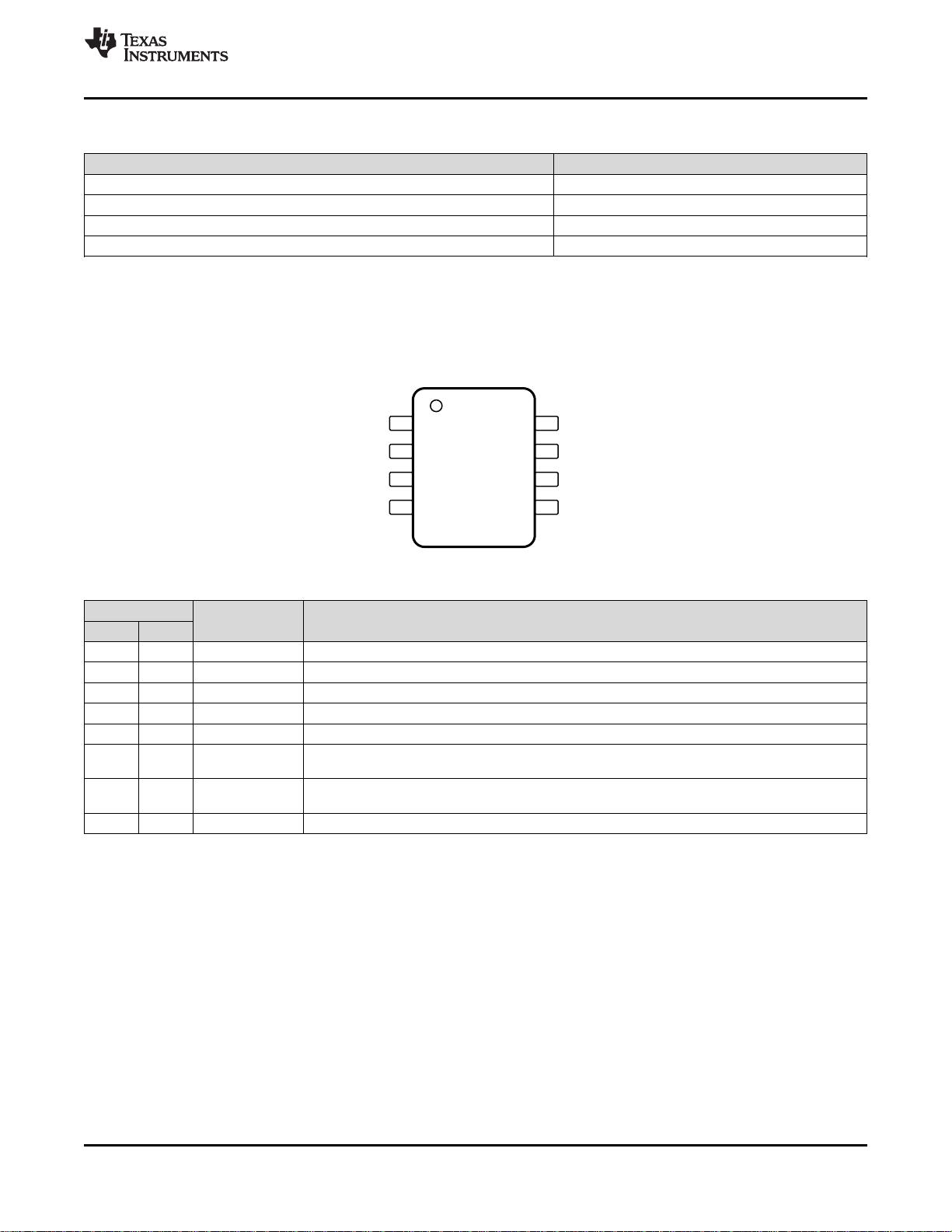
器器件件信信息息
(1)
器器件件型型号号 封封装装 封封装装尺尺寸寸((标标称称值值))
TCA9801 VSSOP (8) 3.00mm × 3.00mm
(1) 如需了解所有可用封装,请参阅数据表末尾的可订购产品附
录。
器器件件比比较较
器器件件型型号号 I
CS
::电电流流源源值值((典典型型
值值))
TCA9800 0.54mA
TCA9801 1.1mA
TCA9802 2.2mA
TCA9803 3.3mA
简简化化原原理理图图

剩余38页未读,继续阅读
资源评论


