没有合适的资源?快使用搜索试试~ 我知道了~
TI-TDP142.pdf
需积分: 11 0 下载量 142 浏览量
2023-02-07
22:56:44
上传
评论 4
收藏 1.64MB PDF 举报
温馨提示
![preview](https://dl-preview.csdnimg.cn/87426230/0001-debcdf51ab67d4acc5d45c1fdf07765a_thumbnail.jpeg)
![preview-icon](https://csdnimg.cn/release/downloadcmsfe/public/img/scale.ab9e0183.png)
试读
37页
DP转接驱动器
资源推荐
资源详情
资源评论
![text/plain](https://img-home.csdnimg.cn/images/20210720083646.png)
![](https://csdnimg.cn/release/download_crawler_static/87426230/bg1.jpg)
TDP142
DP
Receptacle
ML0_IN
ML1_IN
ML2_IN
ML3_IN
ML0_OUT
ML1_OUT
ML2_OUT
ML3_OUT
AUX
HPD
GPU
Copyright © 2017, Texas Instruments Incorporated
GPU
x
TDP142
TDP142
Scaler
Product
Folder
Order
Now
Technical
Documents
Tools &
Software
Support &
Community
本文档旨在为方便起见,提供有关 TI 产品中文版本的信息,以确认产品的概要。 有关适用的官方英文版本的最新信息,请访问 www.ti.com,其内容始终优先。 TI 不保证翻译的准确
性和有效性。 在实际设计之前,请务必参考最新版本的英文版本。
English Data Sheet: SLLSEZ1
TDP142
ZHCSGQ7C –SEPTEMBER 2017–REVISED MAY 2019
TDP142 DisplayPort
TM
8.1Gbps 线线性性转转接接驱驱动动器器
1
1 特特性性
1
• DisplayPort™1.4 高达 8.1Gbps (HBR3)
• 超低功耗架构
• 具有高达 14dB 均衡功能的线性转接驱动器
• 透明呈现 DisplayPort 链路训练
• 可通过 GPIO 或 I
2
C 进行配置
• 支持热插拔
• 支持 DisplayPort 双模标准版本 1.1(交流耦合
HDMI)
• 工业级温度范围:-40ºC 至 85ºC (TDP142I)
• 商业级温度范围:0ºC 至 70ºC (TDP142)
• 4mm x 6mm、0.4mm 间距 WQFN 封装
2 应应用用
• 平板电脑、笔记本电脑、台式电脑、PC
• 有源电缆
• 监视器
• 扩展坞
3 说说明明
TDP142 是一款能够嗅探 AUX 和 HPD 信号的
DisplayPort
TM
(DP) 线性转接驱动器。该器件符合
VESA DisplayPort 标准版本 1.4,支持 1-4 通道主链
路接口,以符合 HBR3 标准的速率(每个通道
8.1Gbps)发送信号。此外,该器件与位置无关。它可
置于源设备、电缆或接收设备内,从而为总体链路预算
有效提供“负损耗”分量。
TDP142 提供多个接收线性均衡级别,用于补偿线缆或
电路板走线中因码间串扰 (ISI) 而产生的损耗。该器件
由 3.3V 单电源供电,支持商业级温度范围 (TDP142)
和工业级温度范围 (TDP142I)。
器器件件信信息息
(1)
器器件件型型号号 封封装装 封封装装尺尺寸寸((标标称称值值))
TDP142 WQFN (40) 4.00mm x 6.00mm
TDP142I WQFN (40) 4.00mm x 6.00mm
(1) 如需了解所有可用封装,请参阅产品说明书末尾的可订购产品
附录。
空白
简简化化电电路路原原理理图图 显显示示屏屏
![](https://csdnimg.cn/release/download_crawler_static/87426230/bg2.jpg)
2
TDP142
ZHCSGQ7C –SEPTEMBER 2017 –REVISED MAY 2019
www.ti.com.cn
Copyright © 2017–2019, Texas Instruments Incorporated
目目录录
1 特特性性.......................................................................... 1
2 应应用用.......................................................................... 1
3 说说明明.......................................................................... 1
4 修修订订历历史史记记录录 ........................................................... 2
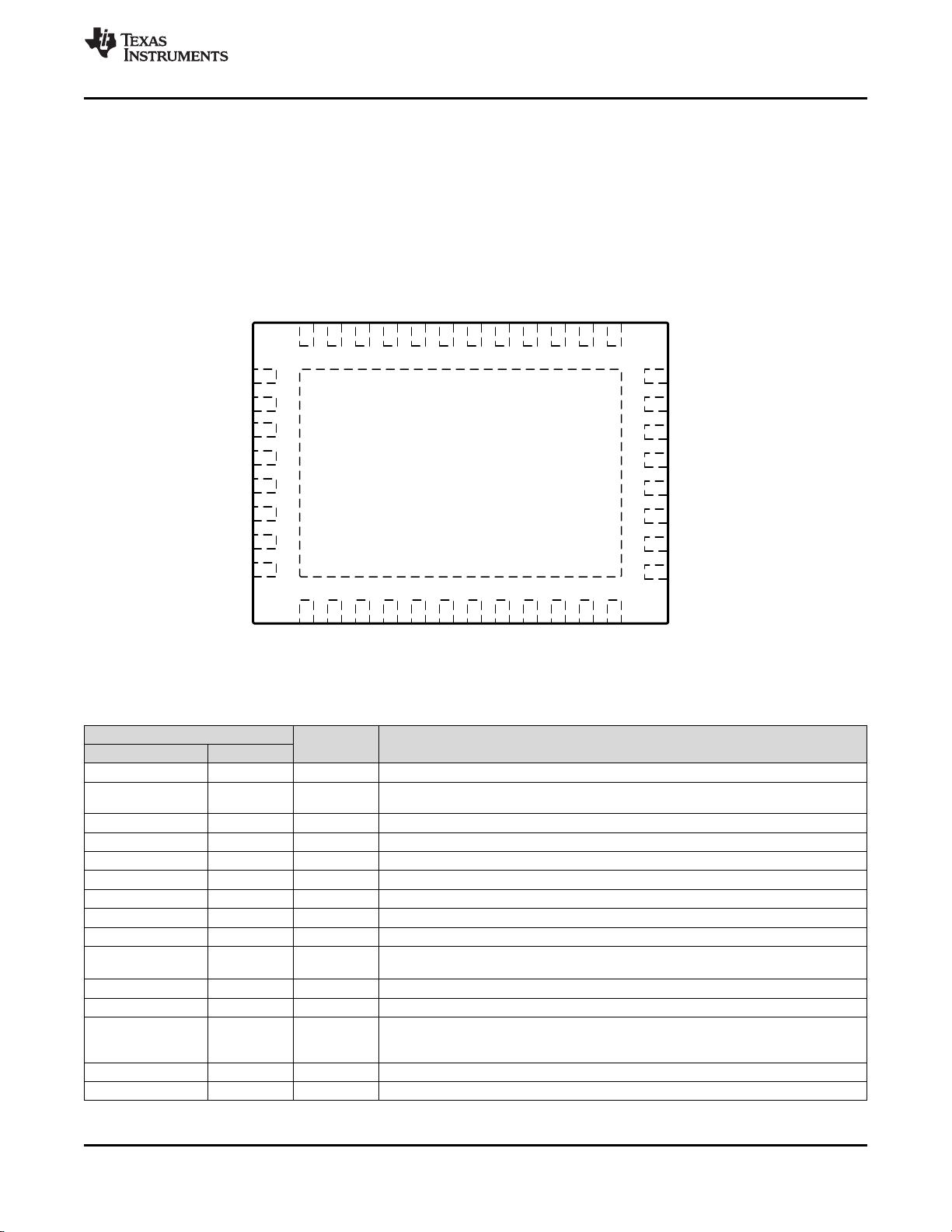
5 Pin Configuration and Functions......................... 3
6 Specifications......................................................... 5
6.1 Absolute Maximum Ratings ...................................... 5
6.2 ESD Ratings.............................................................. 5
6.3 Recommended Operating Conditions....................... 5
6.4 Thermal Information.................................................. 5
6.5 Power Supply Characteristics ................................... 6
6.6 DC Electrical Characteristics .................................... 6
6.7 AC Electrical Characteristics..................................... 7
6.8 Timing Requirements................................................ 8
6.9 Switching Characteristics.......................................... 8
6.10 Typical Characteristics............................................ 9
7 Parameter Measurement Information ................ 10
8 Detailed Description............................................ 11
8.1 Overview ................................................................. 11
8.2 Functional Block Diagram ....................................... 11
8.3 Feature Description................................................. 12
8.4 Device Functional Modes........................................ 13
8.5 Programming........................................................... 15
8.6 Register Maps......................................................... 17
9 Application and Implementation ........................ 20
9.1 Application Information............................................ 20
9.2 Typical Application .................................................. 22
10 Power Supply Recommendations ..................... 25
11 Layout................................................................... 26
11.1 Layout Guidelines ................................................. 26
11.2 Layout Example .................................................... 26
12 器器件件和和文文档档支支持持 ..................................................... 28
12.1 相关链接................................................................ 28
12.2 接收文档更新通知 ................................................. 28
12.3 社区资源................................................................ 28
12.4 商标 ....................................................................... 28
12.5 静电放电警告......................................................... 28
12.6 Glossary................................................................ 28
13 机机械械、、封封装装和和可可订订购购信信息息....................................... 28
4 修修订订历历史史记记录录
Changes from Revision B (August 2018) to Revision C Page
• Added following to pin 11 description: If I2C_EN = “F”, then this pin must be set to “F” or “0”. ........................................... 3
Changes from Revision A (October 2017) to Revision B Page
• Changed the appearance of the pinout image in the Pin Configuration and Function section .............................................. 3
• Added Note 2 To pins 29 and 32 in the Pin Functions table.................................................................................................. 4
Changes from Original (September 2017) to Revision A Page
• Changed the Human-body model (HBM) value From: ±6000 To: ±5000 in the ESD Ratings............................................... 5
![](https://csdnimg.cn/release/download_crawler_static/87426230/bg3.jpg)
Thermal
Pad
1VCC
2DPEQ1
3RSVD1
4RSVD2
5RSVD3
6VCC
7RSVD4
8RSVD5
9INDP0p
10INDP0n
11A0
12INDP1p
13INDP1n
14DPEQ0/A1
15INDP2p
16INDP2n
17I2C_EN
18INDP3p
19INDP3n
20VCC
21 TEST1/SCL
22 TEST2/SDA
23 DPEN/HPDIN
24 AUXp
25 AUXn
26 RSVD6
27 RSVD7
28 VCC
29 SNOOPENZ/RSVD8
30 OUTDP3p
31 OUTDP3n
32 HPDIN/RSVD9
33 OUTDP2p
34 OUTDP2n
35 RSVD10
36 OUTDP1n
37 OUTDP1p
38 RSVD11
39 OUTDP0n
40 OUTDP0p
Not to scale
3
TDP142
www.ti.com.cn
ZHCSGQ7C –SEPTEMBER 2017–REVISED MAY 2019
Copyright © 2017–2019, Texas Instruments Incorporated
(1) Leave unconnected on PCB.
5 Pin Configuration and Functions
RNQ Package
40-Pin (WQFN)
Top View
Pin Functions
PIN
I/O DESCRIPTION
NAME NO.
VCC 1, 6, 20, 28 P 3.3-V Power Supply.
DPEQ1 2 4 Level I
DisplayPort Receiver EQ control. This along with DPEQ0 will select the DisplayPort receiver
equalization gain. Refer to 表 2 for equalization settings.
RSVD1 3 I Reserved.
(1)
RSVD2 4 O Reserved.
(1)
RSVD3 5 O Reserved.
(1)
RSVD4 7 I Reserved.
(1)
RSVD5 8 I Reserved.
(1)
INDP0p 9 I DP Differential positive input for DisplayPort Lane 0.
INDP0n 10 I DP Differential negative input for DisplayPort Lane 0.
A0 11 4 Level I
When I2C_EN = 0, leave the pin unconnected. When I2C_EN is not ‘0’, this pin will also set the
TDP142 I
2
C address. See 表 4. If I2C_EN = “F”, then this pin must be set to “F” or “0”.
INDP1p 12 Diff I DP Differential positive input for DisplayPort Lane 1.
INDP1n 13 Diff I DP Differential negative input for DisplayPort Lane 1.
DPEQ0/A1 14 4 Level I
DisplayPort Receiver EQ control. This along with DPEQ1 will select the DisplayPort receiver
equalization gain. Refer to 表 2 for equalization settings. When I2C_EN is not ‘0’, this pin will also
set the TDP142 I
2
C address. See 表 4.
INDP2p 15 Diff I DP Differential positive input for DisplayPort Lane 2.
INDP2n 16 Diff I DP Differential negative input for DisplayPort Lane 2.
![](https://csdnimg.cn/release/download_crawler_static/87426230/bg4.jpg)
4
TDP142
ZHCSGQ7C –SEPTEMBER 2017 –REVISED MAY 2019
www.ti.com.cn
Copyright © 2017–2019, Texas Instruments Incorporated
Pin Functions (continued)
PIN
I/O DESCRIPTION
NAME NO.
(2) Not a fail-safe I/O. Actively driving pin high while VCC is removed results in leakage voltage on VCC pins.
I2C_EN 17 4 Level I
I
2
C Programming Mode or GPIO Programming Select. I2C is only disabled when this pin is ‘0".
0 = GPIO mode (I
2
C disabled).
R = TI Test Mode (I
2
C enabled at 3.3 V).
F = I
2
C enabled at 1.8 V.
1 = I
2
C enabled at 3.3 V.
INDP3p 18 Diff I DP Differential positive input for DisplayPort Lane 3.
INDP3n 19 Diff I DP Differential negative input for DisplayPort Lane 3.
TEST1/SCL 21 2 Level I
When I2C_EN=’0’, pull down with 10k or directly connect to ground. Otherwise this pin is I
2
C
clock. . When used for I
2
C clock pullup to I
2
C master's VCC I
2
C supply.
TEST2/SDA 22 2 Level I
When I2C_EN=’0’ , pull down with 10k or directly connect to ground. Otherwise this pin is I
2
C data.
When used for I
2
C data pullup to I
2
C master's VCC I
2
C supply.
DPEN/HPDIN 23
2 Level I
(Failsafe)
(PD)
DP Enable Pin. When I2C_EN = ‘0’, this pin will enable or disable DisplayPort functionality.
Otherwise, when I2C_EN is not "0", DisplayPort functionality is enabled and disabled through I
2
C
registers.
L = DisplayPort Disabled. (Pull-down with 10k resistor)
H = DisplayPort Enabled. (Pull-up with10k resistor)
When I2C_EN is not "0" this pin is an input for Hot Plug Detect (HPD) received from DisplayPort
sink. When this HPDIN is low for greater than 2 ms, all DisplayPort lanes are disabled.
AUXp 24 I/O, CMOS
This pin along with AUXN is used by the TDP142 for AUX snooping. See the Application and
Implementation section for more detail.
AUXn 25 I/O, CMOS
This pin along with AUXP is used by the TDP142 for AUX snooping. See the Application and
Implementation section for more detail.
RSVD6 26 I/O, CMOS Reserved.
(1)
RSVD7 27 I/O, CMOS Reserved.
(1)
SNOOPENZ/RSVD8 29
(2)
I/O
(PD)
When I2C_EN ! = 0, this pin is reserved. When I2C_EN = 0 , this pin is SNOOPENZ (L = AUX
snoop enabled and H = AUX snoop disabled with all lanes active).
OUTDP3p 30 Diff O DP Differential positive output for DisplayPort Lane 3.
OUTDP3n 31 Diff O DP Differential negative output for DisplayPort Lane 3.
HPDIN/RSVD9 32
(2)
I/O
(PD)
When I2C_EN ! = 0, this pin is reserved. When I2C_EN = 0, this pin is an input for Hot Plug Detect
received from DisplayPort sink. When HPDIN is low for greater than 2ms, all DisplayPort lanes are
disabled.
OUTDP2p 33 Diff O DP Differential positive output for DisplayPort Lane 2.
OUTDP2n 34 Diff O DP Differential negative output for DisplayPort Lane 2.
RSVD10 35 I Reserved.
(1)
OUTDP1n 36 Diff O DP Differential negative output for DisplayPort Lane 1.
OUTDP1p 37 Diff O DP Differential positive output for DisplayPort Lane 1.
RSVD11 38 I Reserved.
(1)
OUTDP0n 39 Diff O DP Differential negative output for DisplayPort Lane 0.
OUTDP0p 40 Diff O DP Differential positive output for DisplayPort Lane 0.
GND Thermal Pad G Ground.
![](https://csdnimg.cn/release/download_crawler_static/87426230/bg5.jpg)
5
TDP142
www.ti.com.cn
ZHCSGQ7C –SEPTEMBER 2017–REVISED MAY 2019
Copyright © 2017–2019, Texas Instruments Incorporated
(1) Stresses beyond those listed under Absolute Maximum Ratings may cause permanent damage to the device. These are stress ratings
only, which do not imply functional operation of the device at these or any other conditions beyond those indicated under Recommended
Operating Conditions. Exposure to absolute-maximum-rated conditions for extended periods may affect device reliability.
(2) All voltage values are with respect to the GND terminals.
6 Specifications
6.1 Absolute Maximum Ratings
over operating free-air temperature range (unless otherwise noted)
(1)
MIN MAX UNIT
Supply Voltage Range
(2)
, V
CC
–0.3 4 V
Voltage Range at any input or output pin
Differential voltage between positive and
negative inputs
–2.5 2.5 V
Voltage at differential inputs –0.5 V
CC
+ 0.5 V
CMOS Inputs –0.5 V
CC
+ 0.5 V
Maximum junction temperature, T
J
125 °C
Storage temperature, T
stg
–65 150 °C
(1) JEDEC document JEP155 states that 500-V HBM allows safe manufacturing with a standard ESD control process.
(2) JEDEC document JEP157 states that 250-V CDM allows safe manufacturing with a standard ESD control process.
6.2 ESD Ratings
VALUE UNIT
V
(ESD)
Electrostatic discharge
Human-body model (HBM), per ANSI/ESDA/JEDEC JS-001
(1)
±5000
V
Charged-device model (CDM), per JEDEC specification JESD22-
C101
(2)
±1500
6.3 Recommended Operating Conditions
over operating free-air temperature range (unless otherwise noted)
MIN NOM MAX UNIT
V
CC
Main power supply 3 3.3 3.6 V
Supply Ramp Requirement 100 ms
V
(12C)
Supply that external resistors are pulled up to on SDA and SCL 1.7 3.6 V
V
(PSN)
Supply Noise on V
CC
pins 100 mV
T
A
Operating free-air temperature
TDP142 0 70 °C
TDP142I –40 85 °C
(1) For more information about traditional and new thermal metrics, see the Semiconductor and IC Package Thermal Metrics application
report.
6.4 Thermal Information
THERMAL METRIC
(1)
TDP142
UNITRNQ (WQFN)
40 PINS
R
θJA
Junction-to-ambient thermal resistance 37.6 °C/W
R
θJC(top)
Junction-to-case (top) thermal resistance 20.7 °C/W
R
θJB
Junction-to-board thermal resistance 9.5 °C/W
ψ
JT
Junction-to-top characterization parameter 0.2 °C/W
ψ
JB
Junction-to-board characterization parameter 9.4 °C/W
R
θJC(bot)
Junction-to-case (bottom) thermal resistance 2.3 °C/W
剩余36页未读,继续阅读
资源评论
![avatar-default](https://csdnimg.cn/release/downloadcmsfe/public/img/lazyLogo2.1882d7f4.png)
![avatar](https://profile-avatar.csdnimg.cn/107303f5121d47e49d12d0a9ae68af10_weixin_54787054.jpg!1)
不觉明了
- 粉丝: 3278
- 资源: 5614
上传资源 快速赚钱
我的内容管理 展开
我的资源 快来上传第一个资源
我的收益
登录查看自己的收益我的积分 登录查看自己的积分
我的C币 登录后查看C币余额
我的收藏
我的下载
下载帮助
![voice](https://csdnimg.cn/release/downloadcmsfe/public/img/voice.245cc511.png)
![center-task](https://csdnimg.cn/release/downloadcmsfe/public/img/center-task.c2eda91a.png)
安全验证
文档复制为VIP权益,开通VIP直接复制
![dialog-icon](https://csdnimg.cn/release/downloadcmsfe/public/img/green-success.6a4acb44.png)