TI-DS90C124-Q1.pdf

DEN
VODSEL
D
IN
TRFB
24
REN
RRFB
RPWDNB
TCLK
TPWDNB
SERIALIZER ± DS90C241
PLL
Timing
and
Control
D
OUT
-
R
T
=
100
:
R
T
=
100
:
R
IN
-
DESERIALIZER ± DS90C124
D
OUT
+ R
IN
+
PLL
Timing
and
Control
24
R
OUT
LOCK
RCLK
Clock
Recovery
Output Latch
Serial to Parallel
DC Balance Decode
Input Latch
Parallel to Serial
DC Balance Encode
CLK1
bit0
bit1
bit2
bit3
bit4
bit5
bit
6
bit
7
bit
8
bit
9
bit
10
bit
11
DCA
DCB
bit
12
bit
13
bit
14
bit
15
bit
16
bit
17
bit
18
bit
19
bit
20
bit
21
bit
22
bit
23
CLK0
PRE
Copyright © 2017, Texas Instruments Incorporated
Product
Folder
Order
Now
Technical
Documents
Tools &
Software
Support &
Community
An IMPORTANT NOTICE at the end of this data sheet addresses availability, warranty, changes, use in safety-critical applications,
intellectual property matters and other important disclaimers. PRODUCTION DATA.
DS90C124
,
DS90C241
SNLS209M –NOVEMBER 2005–REVISED JANUARY 2017
DS90C241 and DS90C124 5-MHz to 35-MHz DC-Balanced 24-Bit
FPD-Link II Serializer and Deserializer
1
1 Features
1
• 5-MHz to 35-MHz Clock Embedded and DC-
Balancing 24:1 and 1:24 Data Transmissions
• User Defined Pre-Emphasis Driving Ability
Through External Resistor on LVDS Outputs and
Capable to Drive Up to 10-Meter Shielded
Twisted-Pair Cable
• User-Selectable Clock Edge for Parallel Data on
Both Transmitter and Receiver
• Internal DC Balancing Encode and Decode
(Supports AC-Coupling Interface With No External
Coding Required)
• Individual Power-Down Controls for Both
Transmitter and Receiver
• Embedded Clock CDR (Clock and Data Recovery)
on Receiver and No External Source of Reference
Clock Required
• All Codes RDL (Random Data Lock) to Support
Live-Pluggable Applications
• LOCK Output Flag to Ensure Data Integrity at
Receiver Side
• Balanced T
SETUP
and T
HOLD
Between RCLK and
RDATA on Receiver Side
• PTO (Progressive Turnon) LVCMOS Outputs to
Reduce EMI and Minimize SSO Effects
• All LVCMOS Inputs and Control Pins Have
Internal Pulldown
• On-Chip Filters for PLLs on Transmitter and
Receiver
• Temperature Range: –40°C to 105°C
• Greater Than 8-kV HBM ESD Tolerant
• Meets AEC-Q100 Compliance
• Power Supply Range: 3.3 V ± 10%
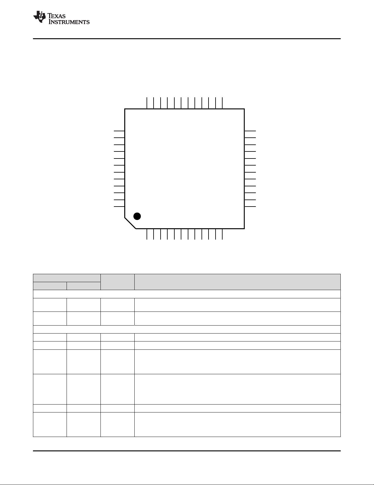
• 48-Pin TQFP Package
2 Applications
• Automotive Central Information Displays
• Automotive Instrument Cluster Displays
• Automotive Heads-Up Displays
• Remote Camera-Based Driver Assistance
Systems
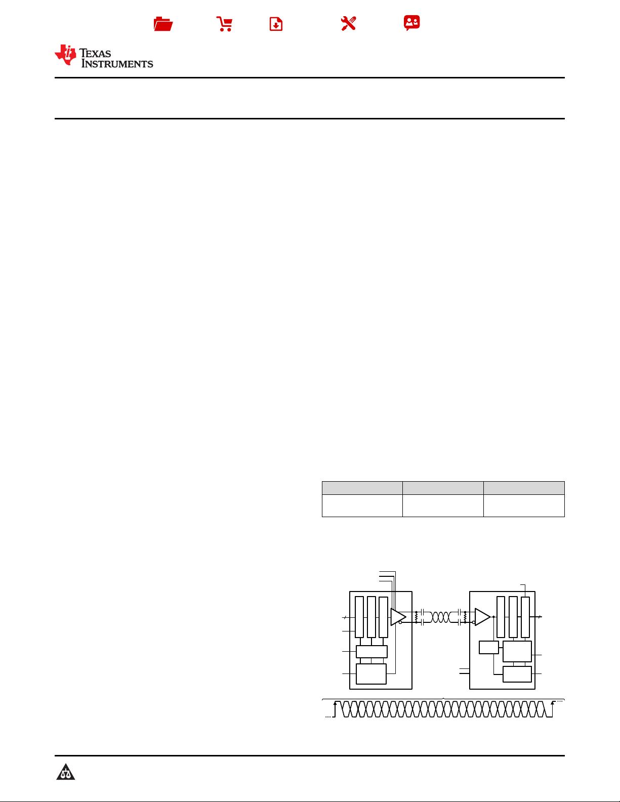
3 Description
The DS90C241 and DS90C124 chipset translates a
24-bit parallel bus into a fully transparent data and
control LVDS serial stream with embedded clock
information. This single serial stream simplifies
transferring a 24-bit bus over PCB traces or over
cable by eliminating the skew problems between
parallel data and clock paths. It saves system cost by
narrowing data paths, which in turn reduces PCB
layers, cable width, and connector size and pins.
The DS90C241 and DS90C124 incorporate LVDS
signaling on the high-speed I/O. LVDS provides a
low-power and low-noise environment for reliably
transferring data over a serial transmission path. By
optimizing the serializer output edge rate for the
operating frequency range, EMI is further reduced.
In addition, the device features pre-emphasis to boost
signals over longer distances using lossy cables.
Internal DC balanced encoding and decoding
supports AC-coupled interconnects.
Device Information
(1)
PART NUMBER PACKAGE BODY SIZE (NOM)
DS90C124
DS90C241
TQFP (48) 7.00 mm x 7.00 mm
(1) For all available packages, see the orderable addendum at
the end of the data sheet.
Block Diagram
剩余39页未读,继续阅读
资源评论

 qq_335607272023-02-02#完美解决问题 #运行顺畅 #内容详尽 #全网独家 #注释完整
- m0_745259962023-02-02#完美解决问题 #运行顺畅 #内容详尽 #全网独家 #注释完整

不觉明了
- 粉丝: 3102
- 资源: 5337


最新资源
- Screenshot_20240427_031602.jpg
- 网页PDF_2024年04月26日 23-46-14_QQ浏览器网页保存_QQ浏览器转格式(6).docx
- 直接插入排序,冒泡排序,直接选择排序.zip
- 在排序2的基础上,再次对快排进行优化,其次增加快排非递归,归并排序,归并排序非递归版.zip
- 实现了7种排序算法.三种复杂度排序.三种nlogn复杂度排序(堆排序,归并排序,快速排序)一种线性复杂度的排序.zip
- 冒泡排序 直接选择排序 直接插入排序 随机快速排序 归并排序 堆排序.zip
- 课设-内部排序算法比较 包括冒泡排序、直接插入排序、简单选择排序、快速排序、希尔排序、归并排序和堆排序.zip
- Python排序算法.zip
- C语言实现直接插入排序、希尔排序、选择排序、冒泡排序、堆排序、快速排序、归并排序、计数排序,并带图详解.zip
- 常用工具集参考用于图像等数据处理
资源上传下载、课程学习等过程中有任何疑问或建议,欢迎提出宝贵意见哦~我们会及时处理!
点击此处反馈


