没有合适的资源?快使用搜索试试~ 我知道了~
TI-DS90C031QML-SP.pdf
需积分: 8 0 下载量 89 浏览量
2023-02-08
22:53:12
上传
评论 4
收藏 722KB PDF 举报
温馨提示
试读
21页
LVDS驱动器
资源推荐
资源详情
资源评论
DS90C031QML
www.ti.com
SNLS202B –MARCH 2006–REVISED MARCH 2013
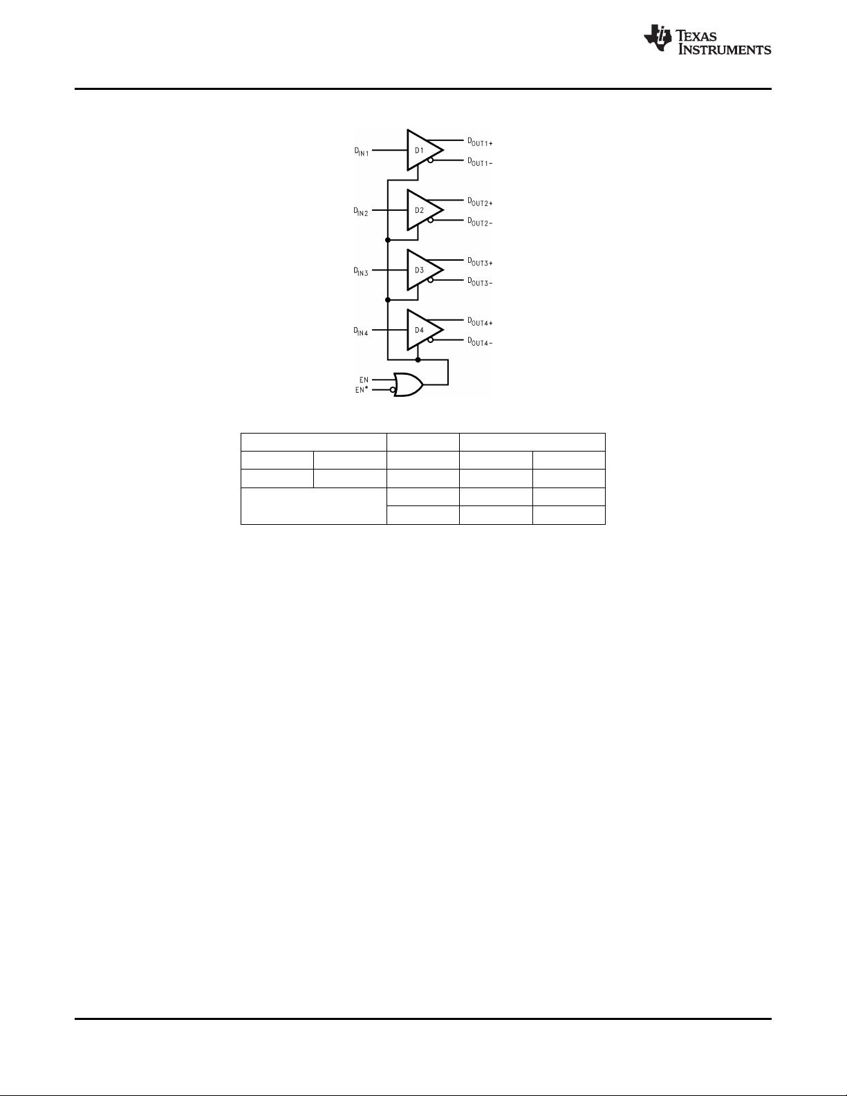
DS90C031QML LVDS Quad CMOS Differential Line Driver
Check for Samples: DS90C031QML
1
FEATURES
DESCRIPTION
The DS90C031 is a quad CMOS differential line
2
• Radiation guaranteed 100 krad(Si)
driver designed for applications requiring ultra low
• High impedance LVDS outputs with power-off
power dissipation and high data rates.
• ±350 mV differential signaling
The DS90C031 accepts TTL/CMOS input levels and
• Low power dissipation
translates them to low voltage (350 mV) differential
• Low differential skew
output signals. In addition the driver supports a TRI-
STATE function that may be used to disable the
• Low propagation delay
output stage, thus dropping the device to a low idle
• Pin compatible with DS26C31
power state of 11 mW typical.
• Compatible with IEEE 1596.3 SCI LVDS
In addition, the DS90C031 provides power-off high
standard
impedance LVDS outputs. This feature assures
• Compatible with proposed TIA LVDS standard
minimal loading effect on the LVDS bus lines when
V
CC
is not present. The DS90C031 and companion
• Fail safe logic for floating inputs
line receiver (DS90C032) provide a new alternative to
high power psuedo-ECL devices for high speed point-
to-point interface applications.
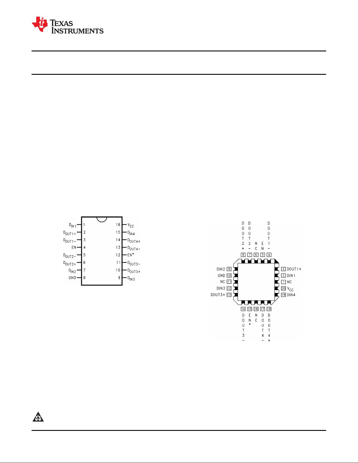
Connection Diagram
Figure 1. Dual-In-Line
See Package Number NAD0016A & NAC0016A
Figure 2. LCCC Package
See Pacakage Number NAJ0020A
1
Please be aware that an important notice concerning availability, standard warranty, and use in critical applications of
Texas Instruments semiconductor products and disclaimers thereto appears at the end of this data sheet.
2All trademarks are the property of their respective owners.
PRODUCTION DATA information is current as of publication date.
Copyright © 2006–2013, Texas Instruments Incorporated
Products conform to specifications per the terms of the Texas
Instruments standard warranty. Production processing does not
necessarily include testing of all parameters.
DS90C031QML
SNLS202B –MARCH 2006–REVISED MARCH 2013
www.ti.com
Functional Block Diagram
Truth Table
Enables Input Outputs
EN EN* D
I
D
O+
D
O−
L H X Z Z
L L H
All other combinations of
ENABLE inputs
H H L
2 Submit Documentation Feedback Copyright © 2006–2013, Texas Instruments Incorporated
Product Folder Links: DS90C031QML
DS90C031QML
www.ti.com
SNLS202B –MARCH 2006–REVISED MARCH 2013
These devices have limited built-in ESD protection. The leads should be shorted together or the device placed in conductive foam
during storage or handling to prevent electrostatic damage to the MOS gates.
Absolute Maximum Ratings
(1)
Supply Voltage (V
CC
) −0.3V to +6V
Input Voltage (D
I
) −0.3V to (V
CC
+ 0.3V)
Enable Input Voltage (EN, EN*) −0.3V to (V
CC
+ 0.3V)
Output Voltage (D
O+
, D
O−
) −0.3V to + 5.8V
Storage Temperature Range −65°C ≤ T
A
≤ +150°C
Lead Temperature Range, Soldering (4 seconds) +260°C
Maximum Package Power Dissipation at +25°C
(2)
20 Pin LCCC Package 1900 mW
16 Pin CLGA (NAD) 1450 mW
16 Pin CLGA (NAC) 1450 mW
Thermal Resistance
θ
JA
20 Pin LCCC Package 78°C/W
16 Pin CLGA (NAD) 145°C/W
16 Pin CLGA (NAC) 145°C/W
θ
JC
20 Pin LCCC Package 18°C/W
16 Pin CLGA (NAD) 14°C/W
16 Pin CLGA (NAC) 14°C/W
ESD Rating
(3)
3.5KV
(1) Absolute Maximum Ratings indicate limits beyond which damage to the device may occur. Operating Ratings indicate conditions for
which the device is functional, but do not guarantee specific performance limits. For guaranteed specifications and test conditions, see
the Electrical Characteristics. The guaranteed specifications apply only for the test conditions listed. Some performance characteristics
may degrade when the device is not operated under the listed test conditions.
(2) Derate LCCC at 12.8mW/°C above +25°C. Derate CLGA at 6.9mW/°C above +25°C.
(3) Human body model, 1.5 kΩ in series with 100 pF.
Recommended Operating Conditions
Min Typ Max Unit
Supply Voltage (V
CC
) +4.5 +5.0 +5.5 V
Operating Free Air Temperature (T
A
) −55 +25 +125 °C
Copyright © 2006–2013, Texas Instruments Incorporated Submit Documentation Feedback 3
Product Folder Links: DS90C031QML
DS90C031QML
SNLS202B –MARCH 2006–REVISED MARCH 2013
www.ti.com
Quality Conformance Inspection
Table 1. Mil-Std-883, Method 5005 - Group A
Subgroup Description Temp (°C)
1 Static tests at +25
2 Static tests at +125
3 Static tests at -55
4 Dynamic tests at +25
5 Dynamic tests at +125
6 Dynamic tests at -55
7 Functional tests at +25
8A Functional tests at +125
8B Functional tests at -55
9 Switching tests at +25
10 Switching tests at +125
11 Switching tests at -55
12 Settling time at +25
13 Settling time at +125
14 Settling time at -55
DC Parameters
(1)
Sub-
Symbol Parameter Conditions Notes Min Max Units
groups
V
OD1
Differential Ouput Voltage R
L
= 100Ω 250 450 mV 1, 2, 3
DV
OD1
Change in Magnitude of Vod1 for R
L
= 100Ω 35 mV 1, 2, 3
complementary output States
V
OS
Offset Voltage R
L
= 100Ω 1.12 1.37 V 1, 2, 3
5 5
DV
OS
Change in Magnitude of Vos for R
L
= 100Ω 25 mV 1, 2, 3
Complementary Output States
V
OH
Output Voltage High R
L
= 100Ω 1.6 V 1, 2, 3
V
OL
Output Voltage Low R
L
= 100Ω 0.9 V 1, 2, 3
V
IH
Input Voltage High
(2)
2.0 V
CC
V 1, 2, 3
V
IL
Input Voltage Low
(2)
Gnd 0.8 V 1, 2, 3
I
I
Input Current V
I
= V
CC
, Gnd, 2.5, or 0.4V ±10 µA 1, 2, 3
V
Cl
Input Clamp Voltage I
Cl
= -18mA -1.5 V 1, 2, 3
I
OS
Output Short Circuit Current V
O
= 0V -5.0 mA 1, 2, 3
I
Off
Power-off Leakage V
O
= 0V or 2.4V, ±10 µA 1, 2, 3
V
CC
-= 0V or Open
I
OZ
Output TRI-STATE Current EN = 0.8V and EN* = 2.0V ±10 µA 1, 2, 3
V
O
= 0V or V
CC
I
CC
Drivers Enabled Supply Current D
I
= Hi or Low 25 mA 1, 2, 3
I
CCZ
Drivers Disabled Supply Current D
I
= Hi or Low, En = Gnd, 10 mA 1, 2, 3
En* = V
CC
(1) Pre and Post irradiation limits are identical to those listed under AC and DC electrical characteristics except as listed in the “Post
Radiation Limits” table. Radiation end point limits for the noted parameters are guaranteed only for the conditions, as specified.
(2) Tested during V
OH
/ V
OL
tests.
4 Submit Documentation Feedback Copyright © 2006–2013, Texas Instruments Incorporated
Product Folder Links: DS90C031QML
DS90C031QML
www.ti.com
SNLS202B –MARCH 2006–REVISED MARCH 2013
AC Parameters
The following conditions apply, unless otherwise specified.
AC: V
CC
= 4.5V / 5.0V / 5.5V, R
L
= 100Ω (between outputs), C
L
= 20pF (each output to Gnd)
Sub-
Symbol Parameter Conditions Notes Min Max Units
groups
t
PHLD
Differential Propagation Delay 0.5 5.0 ns 9, 10, 11
High to Low
t
PLHD
Differential Propagation Delay 0.5 5.0 ns 9, 10, 11
Low to High
t
SkD
Differential Skew |tPHLD-tPLHD| 3.0 ns 9, 10, 11
t
Sk1
Channel to Channel Skew
(1)
3.0 ns 9, 10, 11
t
Sk2
Chip to Chip Skew
(2)
4.5 ns 9, 10, 11
t
PHZ
Disable Time High to Z
(3)
20 ns 9, 10, 11
t
PLZ
Disable Time Low To Z
(3)
20 ns 9, 10, 11
t
PZH
Enable Time Z to High
(3)
20 ns 9, 10, 11
t
PZL
Enable Time Z to Low
(3)
20 ns 9, 10, 11
(1) Channel-to-Channel Skew is defined as the difference between the propagation delay of the channel and the other channels in the
same chip with an event on the inputs.
(2) Chip to Chip Skew is defined as the difference between the minimum and maximum specified differential propagation delays.
(3) Parameter guaranteed, not tested 100%
AC/DC Parameters - Post Radiation Limits
(1)
Sub-
Symbol Parameter Conditions Notes Min Max Units
groups
I
CC
Drivers Enabled Supply Current D
I
- Hi or Low, En = Gnd, 30 mA 1
En* = V
CC
I
CCZ
Drivers Disabled Supply Current D
I
- Hi or Low, En = Gnd, 30 mA 1
En* = V
CC
(1) Pre and Post irradiation limits are identical to those listed under AC and DC electrical characteristics except as listed in the “Post
Radiation Limits” table. Radiation end point limits for the noted parameters are guaranteed only for the conditions, as specified.
Copyright © 2006–2013, Texas Instruments Incorporated Submit Documentation Feedback 5
Product Folder Links: DS90C031QML
剩余20页未读,继续阅读
资源评论
不觉明了
- 粉丝: 3078
- 资源: 5252
上传资源 快速赚钱
- 我的内容管理 展开
- 我的资源 快来上传第一个资源
- 我的收益 登录查看自己的收益
- 我的积分 登录查看自己的积分
- 我的C币 登录后查看C币余额
- 我的收藏
- 我的下载
- 下载帮助
安全验证
文档复制为VIP权益,开通VIP直接复制
信息提交成功