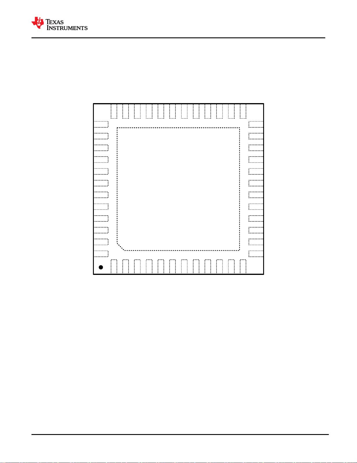
表 5-1. Pin Functions (continued)
PIN I/O
TYPE
(1)
DESCRIPTION
NAME NO.
I2C_SCL 2 I/O, OD
I2C Serial Clock: Clock line for the bidirectional control bus communication.
External 2-kΩ to 4.7-kΩ pullup resistor to 1.8-V or 3.3-V supply rail recommended
per I2C interface standards. I2C_SCL and I2C_SDA inputs are 3.3-V tolerant. See
节
7.5.1 for more information.
I2C_SDA 1 I/O, OD
I2C Serial Data: Data line for bidirectional control bus communication.
External 2-kΩ to 4.7-kΩ pullup resistor to 1.8-V or 3.3-V supply rail recommended
per I2C interface standards. I2C_SCL and I2C_SDA inputs are 3.3-V tolerant. See
节
7.5.1 for more information.
CONFIGURATION AND CONTROL PINS
VDD_SEL 46 S, PD
VDD Select: Configuration pin to select internal LDO regulator supply. When
VDD_SEL = LOW, internal 1.1-V supply mode is selected. Feed 1.8 V to VDD18
inputs = 1.8 V ±5%. An internal 1.1-V regulator will supply the VDD11. VDD11
inputs should be terminated with bypass capacitors. When VDD_SEL = HIGH,
external 1.1-V supply mode is selected. After 1.8-V supply is applied to VDD18
inputs, then apply 1.1 V to VDD11 inputs = 1.1 V ±5%. Voltage at VDD11 supply
pins must always be less than main voltage applied to VDD18 when using
external 1.1-V supply.
IDX 35 S, PD
Input. I2C Serial Control Bus Primary Device ID Address Select.
Once enabled the voltage at this pin will be sampled to configure the default I2C
device address. Typically connected with external pullup resistor to VDD18 and
pulldown resistor to GND to create a voltage divider. See 表 7-15.
MODE 37 S, PD
Mode select configuration input to set operating mode based on input voltage level.
Typically connected to voltage divider through external pullup to VDD18 and
pulldown to GND. See 表 7-1.
PDB 30 I, PD
Power-down inverted Input Pin. Typically connected to processor GPIO with pull
down. When PDB input is brought HIGH, the device is enabled and internal register
and state machines are reset to default values. Asserting PDB signal low will power
down the device and consume minimum power with CSI-2 Tx outputs in tri-state.
The default function of this pin is PDB = LOW; POWER DOWN with internal 50 kΩ
pull down enabled. PDB should remain low until after power supplies are applied
and reach minimum required levels. PDB INPUT IS 3.3-V TOLERANT. See section
节
9.2.
PDB > 1.5 V, device is enabled (normal operation)
PDB = 0, device is powered down.
DIAGNOSTIC PINS
CMLOUTP 38
O
Monitor Loop-Through Driver differential output. Typically routed to test points and
not connected. For monitoring, CMLOUT should be terminated with 100-Ω
differential load. See
节
7.4.10.
CMLOUTN 39
BISTEN 6 S, PD
BIST Enable: BISTEN = H, BIST Mode is enabled BISTEN = L, BIST Mode is
disabled. If unused connect BISTEN directly to GND. See BIST section
节
7.5.12
for more information.
PASS 47 O
PASS Output: PASS = H indicates pass conditions are met and PASS = L signals or
more pass condition is not met. Typically route to processor input pin or test point
for monitoring. May also be configured to indicate logical AND of pass status when
both Rx ports are enabled. See
节
7.4.7 for more information. For BIST operation
PASS = H, ERROR FREE Transmission in forward channel operation. PASS = L,
one or more errors were detected in the received payload. See BIST section for
more information. Leave No Connect if unused.
LOCK 48 O
LOCK Status: Output Pin for monitoring lock status of V
3
Link channel, may be used
as Link Status. LOCK = H, the V
3
Link receiver is Locked and Rx Ports are active.
LOCK = L, receiver is unlocked. May also be configured to indicate logical AND of
lock status when both Rx ports are enabled. See
节
7.4.7 for more information.
Leave No Connect if unused.
RES 44 PD RES must be tied to GND for normal operation.
POWER AND GROUND
www.ti.com.cn
TDES954
ZHCSNJ7 – APRIL 2021
Copyright © 2021 Texas Instruments Incorporated
Submit Document Feedback
5
Product Folder Links: TDES954


 我的内容管理
展开
 我的资源
快来上传第一个资源
 我的收益 登录查看自己的收益
 我的积分
登录查看自己的积分
 我的C币
登录后查看C币余额
 我的收藏
我的收藏  我的下载
我的下载  下载帮助
下载帮助 
 前往需求广场,查看用户热搜

 信息提交成功