TI-TMS28F200BZB.pdf
需积分: 0 142 浏览量
2022-12-10
23:13:45
上传
评论 4
收藏 406KB PDF 举报

TMS28F200BZT, TMS28F200BZB
262144 BY 8-BIT/131072 BY 16-BIT
BOOT-BLOCK FLASH MEMORIES
SMJS200E – JUNE 1994 – REVISED JANUARY 1998
1
POST OFFICE BOX 1443 • HOUSTON, TEXAS 77251–1443
D
Organization... 262144 by 8 bits
131072 by 16 bits
D
Array-Blocking Architecture
– Two 8K-Byte Parameter Blocks
– One 96K-Byte Main Block
– One 128K-Byte Main Block
– One 16K-Byte Protected Boot Block
– Top or Bottom Boot Locations
D
All Inputs/Outputs TTL Compatible
D
Maximum Access/Minimum Cycle Time
V
CC
± 10%
’28F200BZx70 70 ns
’28F200BZx80 80 ns
’28F200BZx90 90 ns
(x = top (T) or bottom (B) boot-block
configurations ordered)
D
10000 Program/Erase-Cycles
D
Three Temperature Ranges
– Commercial...0°C to 70°C
– Extended...– 40°C to 85°C
– Automotive...– 40°C to 125°C
D
Low Power Dissipation (V
CC
= 5.5 V)
– Active Write . . . 330 mW (Byte-Write)
– Active Read...330 mW (Byte-Read)
– Active Write . . . 358 mW (Word-Write)
– Active Read...330 mW (Word-Read)
– Block-Erase...165 mW
– Standby...0.55 mW (CMOS-Input
Levels)
– Deep Power-Down Mode...0.0066 mW
D
Fully Automated On-Chip Erase and
Word/Byte-Program Operations
D
Write-Protection for Boot Block
D
Industry-Standard Command State Machine
(CSM)
– Erase-Suspend/Resume
– Algorithm-Selection Identifier
description
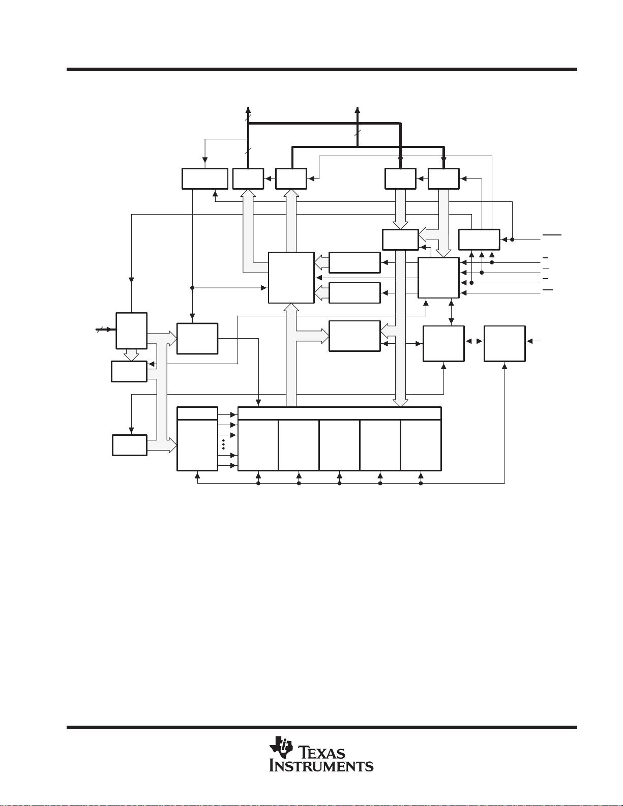
The TMS28F200BZx is a 262144 by 8-bit/131072 by 16-bit (2097152-bit), boot-block flash memory that can
be electrically block-erased and reprogrammed. The TMS28F200BZx is organized in a blocked architecture
consisting of one 16K-byte protected boot block, two 8K-byte parameter blocks, one 96K-byte main block, and
one 128K-byte main block. The device can be ordered with either a top or bottom boot-block configuration.
Operation as a 256K-by 8-bit or a 128K-by16-bit organization is user-definable.
Please be aware that an important notice concerning availability, standard warranty, and use in critical applications of
Texas Instruments semiconductor products and disclaimers thereto appears at the end of this data sheet.
23
V
CC
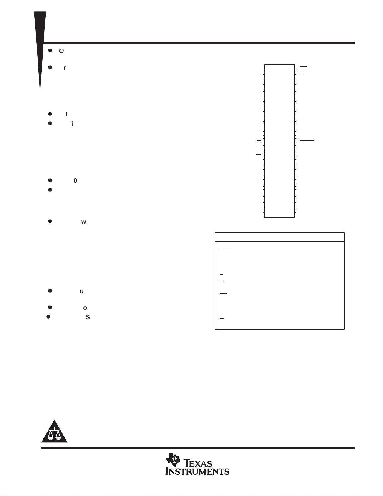
PIN NOMENCLATURE
A0–A16 Address Inputs
BYTE Byte Enable
DQ0–DQ14 Data In/ Out
DQ15/A
–1
Data In/ Out (word-wide mode),
Low-Order Address (byte-wide mode)
E
Chip Enable
G
Output Enable
NC No Internal Connection
RP
Reset/Deep Power-Down
V
CC
5-V Power Supply
V
PP
12-V Power Supply for Program/ Erase
V
SS
Ground
W
Write Enable
DBJ PACKAGE
(TOP VIEW)
V
PP
NC
NC
A7
A6
A5
A4
A3
A2
A1
A0
E
V
SS
G
DQ0
DQ8
DQ1
DQ9
DQ2
DQ10
RP
W
A8
A9
A10
A11
A12
A13
A14
A15
A16
BYTE
V
SS
DQ15/A
–1
DQ7
DQ14
DQ6
DQ13
DQ5
DQ12
1
2
3
4
5
6
7
8
9
10
11
12
13
14
15
16
17
18
44
43
42
41
40
39
38
37
36
35
34
33
32
31
30
29
28
27
19
20
26
25
DQ3
DQ11
DQ4
21
22
24
PRODUCTION DATA information is current as of publication date.
Products conform to specifications per the terms of Texas Instruments
standard warranty. Production processing does not necessarily include
testing of all parameters.
Copyright 1998, Texas Instruments Incorporated


剩余28页未读,继续阅读


评论0
最新资源