Vanguard-VS3080AP.pdf
需积分: 9 152 浏览量
2022-12-10
21:39:49
上传
评论 4
收藏 245KB PDF 举报

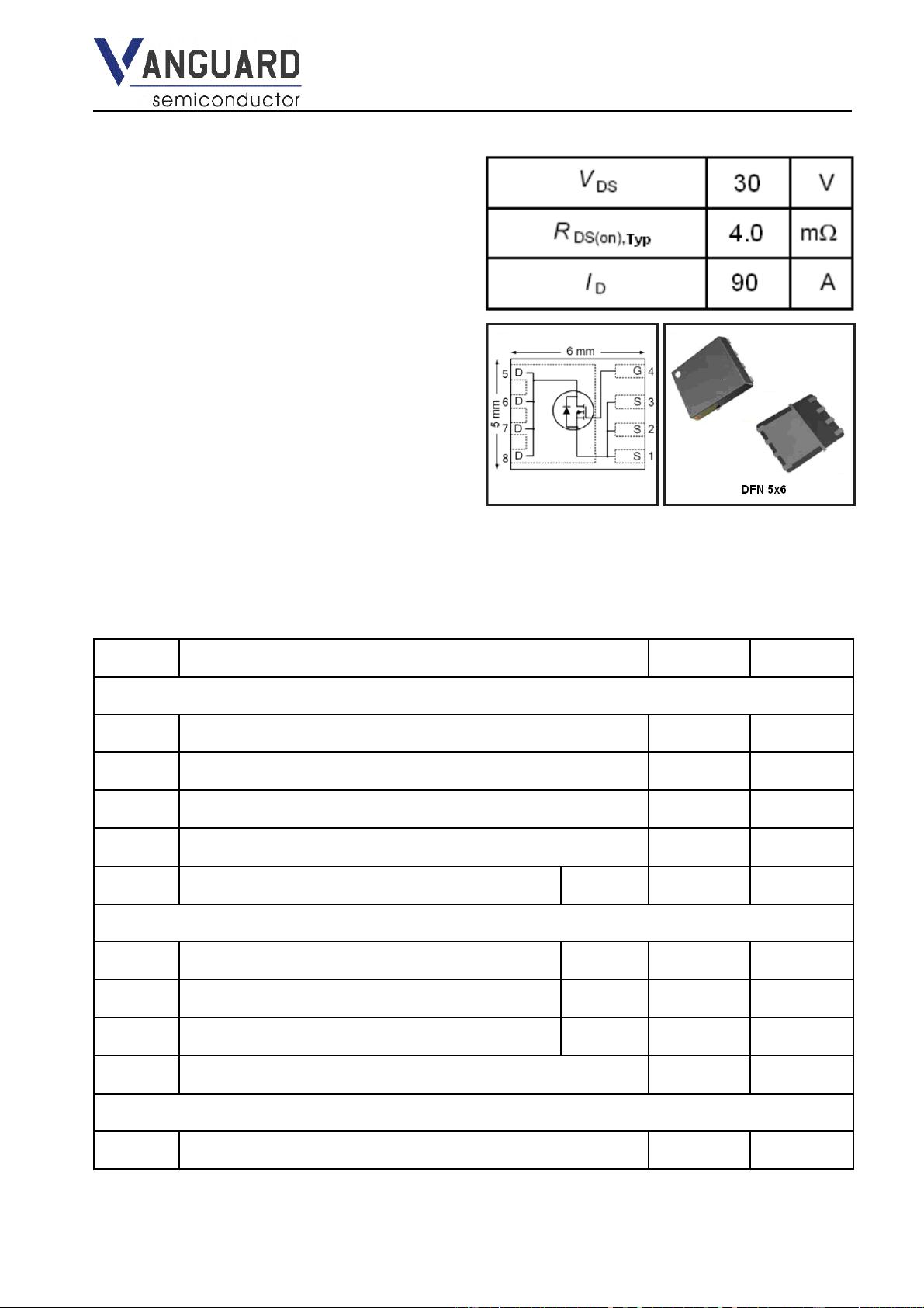
30V/90A N-Channel Advanced Power MOSFET
Copyright© Vanguard Semiconductor Co., Ltd Page 1 of 5
Rev. A– Jun.16
th
, 2013 www.vgsemi.com
VS3080AP
Absolute Maximum Ratings
Stresses beyond those listed under “Absolute Maximum Ratings” may cause permanent damage to the device. These are stress ratings only;and
functional operation of the device at these or any other condition beyond those indicated in the specifications is not implied. Exposure to
absolute-maximum-rated conditions for extended periods may affect device reliability. The thermal resistance and power dissipation ratings are
measured under board mounted and still air conditions. Ambient temperature (TA) is 25°C, unless otherwise specified.
Symbol Parameter Rating Unit
Common Ratings (TC=25°C Unless Otherwise Noted)
VGS Gate-Source Voltage ±20 V
(BR)DSS
V
Drain-Source Breakdown Voltage 30 V
J
T
Maximum Junction Temperature 150 °C
STG
T
Storage Temperature Range -55 to 150 °C
S
I
Diode Continuous Forward Current
C
T
=25°C
90 A
Mounted on Large Heat Sink
DM
I
Pulse Drain Current Tested (Sillicon Limit)
C
T
=25°C
320 A
D
I
Continuous Drain current@V
GS=10V (See Fig2)
C
T
=25°C
90 A
D
P
Maximum Power Dissipation
C
T
=25°C
62 W
θ
JC
R
Thermal Resistance-Junction to Case 1.98 °C/W
Drain-Source Avalanche Ratings
EAS
Avalanche Energy, Single Pulsed ②
225 mJ
Features
♦ Low On-Resistance
♦ Fast Switching
♦ 100% Avalanche Tested
♦ Repetitive Avalanche Allowed up to Tjmax
♦ Lead-Free, RoHS Compliant
Description
VS3080AP designed by the trench processing
techniques to achieve extremely low on-resistance.
Additional features of this design are a 150°C
junction operating temperature, fast switching
speed and improved repetitive avalanche rating .
These features combine to make this design an
extremely efficient and reliable device for use in
Motor applications and a wide variety of other
applications.
资源评论


