TI-TS3V330.pdf
需积分: 9 21 浏览量
2022-12-01
23:44:31
上传
评论 4
收藏 1.48MB PDF 举报

www.ti.com
FEATURES
D
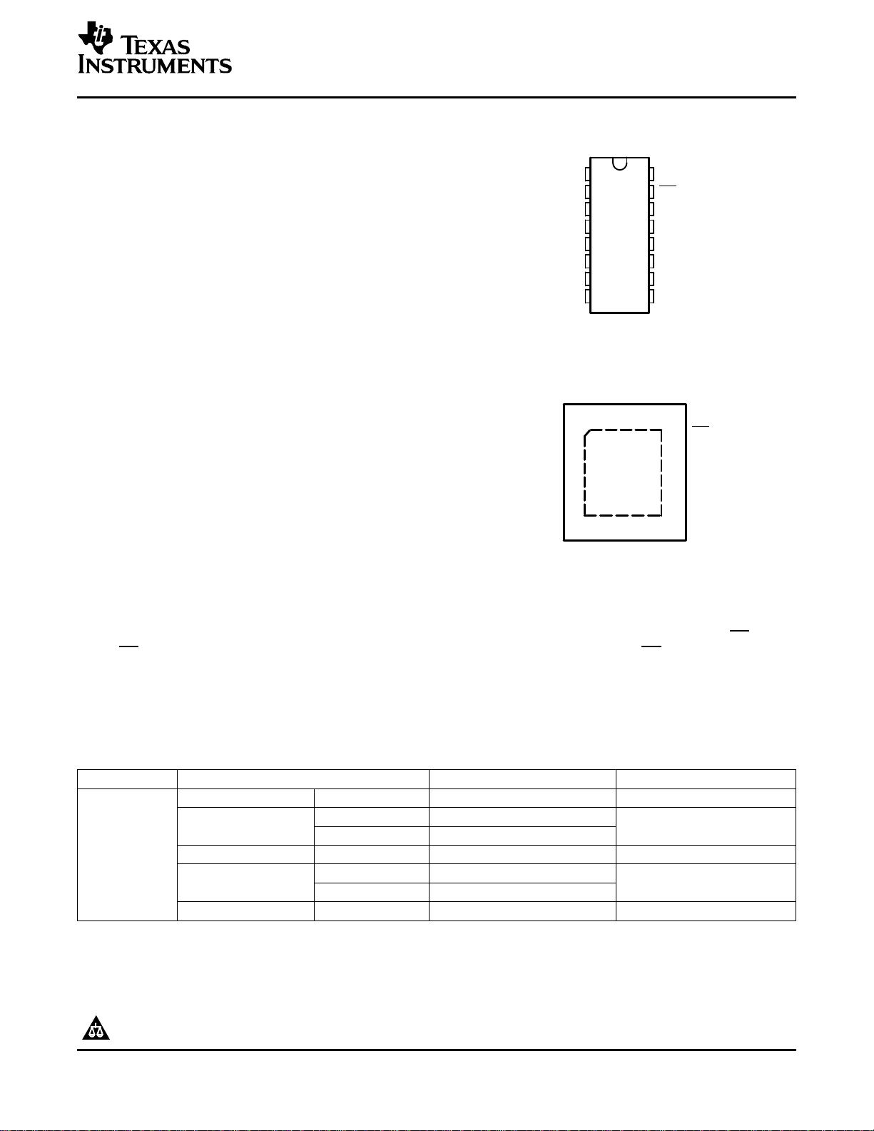
D, DBQ, DGV, OR PW PACKAGE
(TOP VIEW)
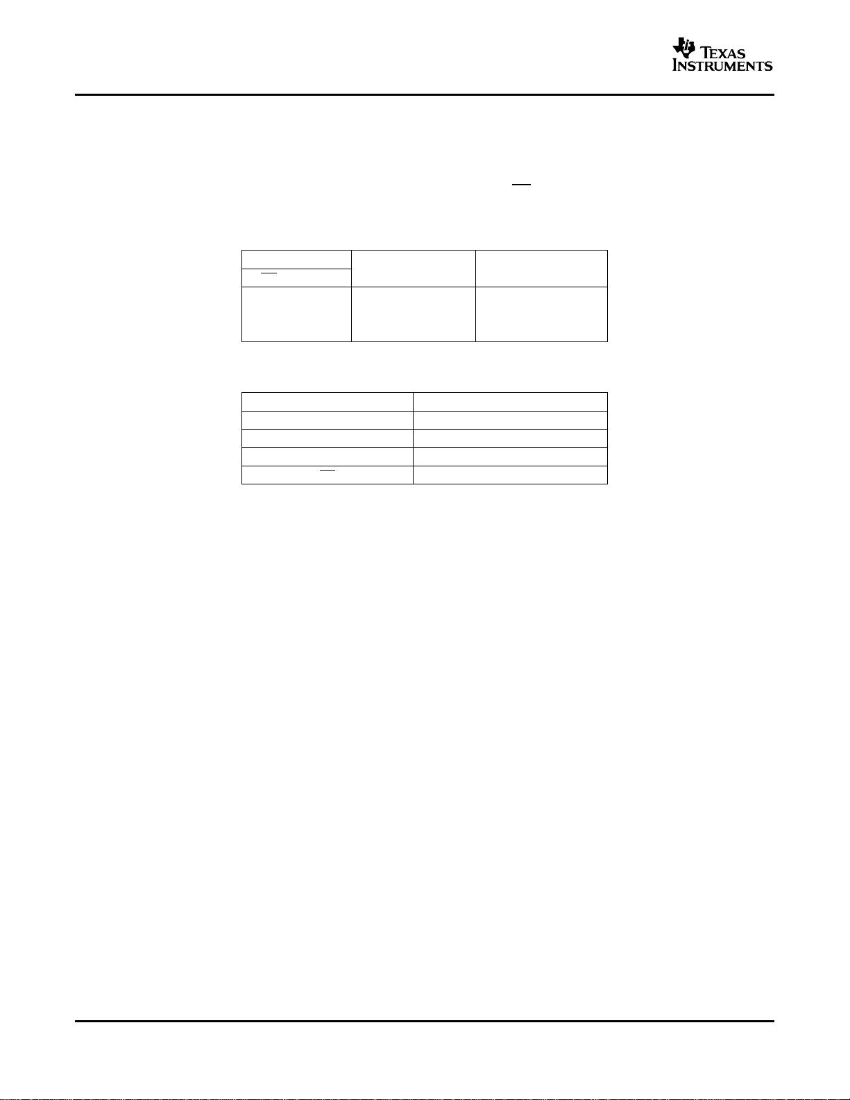
RGY PACKAGE
(TOP VIEW)
1 16
8 9
2
3
4
5
6
7
15
14
13
12
11
10
EN
S1
D
S2
D
D
D
S1
C
S2
C
S1
A
S2
A
D
A
S1
B
S2
B
D
B
IN
V
GND
CC
1
2
3
4
5
6
7
8
16
15
14
13
12
11
10
9
IN
S1
A
S2
A
D
A
S1
B
S2
B
D
B
GND
V
CC
EN
S1
D
S2
D
D
D
S1
C
S2
C
D
C
C
DESCRIPTION/ORDERING INFORMATION
TS3V330
QUAD SPDT WIDE-BANDWIDTH VIDEO SWITCH
WITH LOW ON-STATE RESISTANCE
SCDS162C – MAY 2004 – REVISED JULY 2005
• Low Differential Gain and Phase (D
G
= 0.82%,
D
P
= 0.1 Degree Typ)
• Wide Bandwidth (BW = 300 MHz Min)
• Low Crosstalk (X
TALK
= –80 dB Typ)
• Low Power Consumption
(I
CC
= 10 µ A Max)
• Bidirectional Data Flow With Near-Zero
Propagation Delay
• Low ON-State Resistance (r
on
= 3 Ω Typ)
• Rail-to-Rail Switching on Data I/O Ports
(0 to V
CC
)
• V
CC
Operating Range From 3 V to 3.6 V
• I
off
Supports Partial-Power-Down Mode
Operation
• Data and Control Inputs Provide Undershoot
Clamp Diode
• Latch-Up Performance Exceeds 100 mA Per
JESD 78, Class II
• ESD Performance Tested Per JESD 22
– 2000-V Human-Body Model
(A114-B, Class II)
– 1000-V Charged-Device Model (C101)
• Suitable for Both RGB and Composite-Video
Switching
The TS3V330 video switch is a 4-bit 1-of-2 multiplexer/demultiplexer, with a single switch-enable ( EN) input.
When EN is low, the switch is enabled and the D port is connected to the S port. When EN is high, the switch is
disabled and the high-impedance state exists between the D and S ports. The select (IN) input controls the data
path of the multiplexer/demultiplexer.
Low differential gain and phase make this switch ideal for composite and RGB video applications. This device
has wide bandwidth and low crosstalk, making it suitable for high-frequency applications as well.
ORDERING INFORMATION
T
A
PACKAGE
(1)
ORDERABLE PART NUMBER TOP-SIDE MARKING
QFN – RGY Tape and reel TS3V330RGYR TF330
Tube TS3V330D
SOIC – D TS3V330
Tape and reel TS3V330DR
–40 ° C to 85 ° C SSOP (QSOP) – DBQ Tape and reel TS3V330DBQR TF330
Tube TS3V330PW
TSSOP – PW TF330
Tape and reel TS3V330PWR
TVSOP – DGV Tape and reel TS3V330DGVR TF330
(1) Package drawings, standard packing quantities, thermal data, symbolization, and PCB design guidelines are available at
www.ti.com/sc/package.
Please be aware that an important notice concerning availability, standard warranty, and use in critical applications of Texas
Instruments semiconductor products and disclaimers thereto appears at the end of this data sheet.
PRODUCTION DATA information is current as of publication date.
Copyright © 2004–2005, Texas Instruments Incorporated
Products conform to specifications per the terms of the Texas
Instruments standard warranty. Production processing does not
necessarily include testing of all parameters.

剩余29页未读,继续阅读


评论0
最新资源