TI-OPA1S2385.pdf
需积分: 5 73 浏览量
2022-11-26
21:44:03
上传
评论 4
收藏 1.78MB PDF 举报

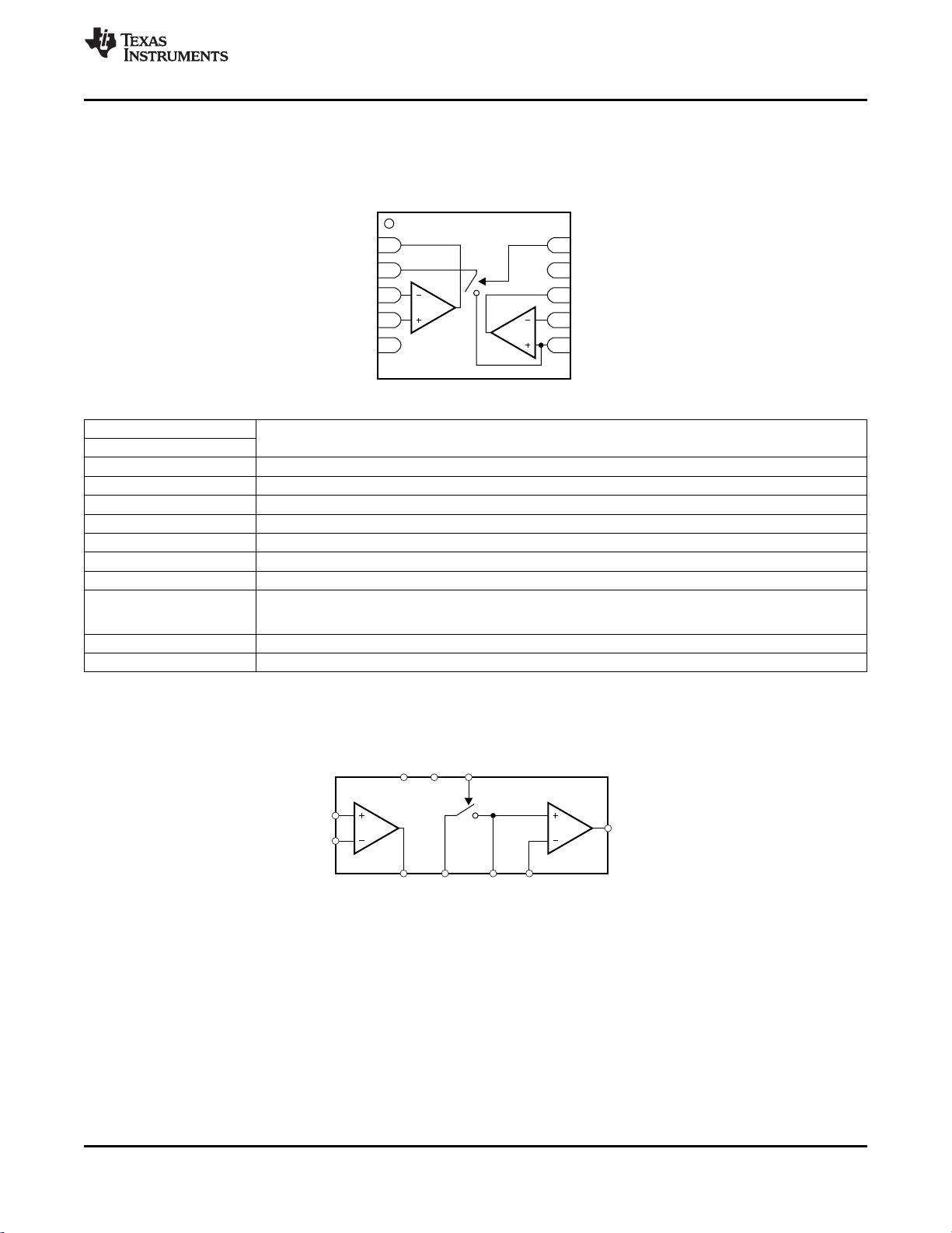
OPA1S2384/5
A
OUT A
-IN A
+IN A
B
IN S +IN B -IN B
V-
V+ SC
(1)
OUT B
OPA1S2384
OPA1S2385
www.ti.com.cn
ZHCSAM4A –DECEMBER 2012–REVISED JUNE 2013
具具有有集集成成开开关关和和缓缓冲冲器器的的 250MHz,,CMOS 转转阻阻放放大大器器 (TIA)
查查询询样样品品: OPA1S2384, OPA1S2385
1
特特性性
说说明明
2
• 宽宽带带宽宽::250MHz
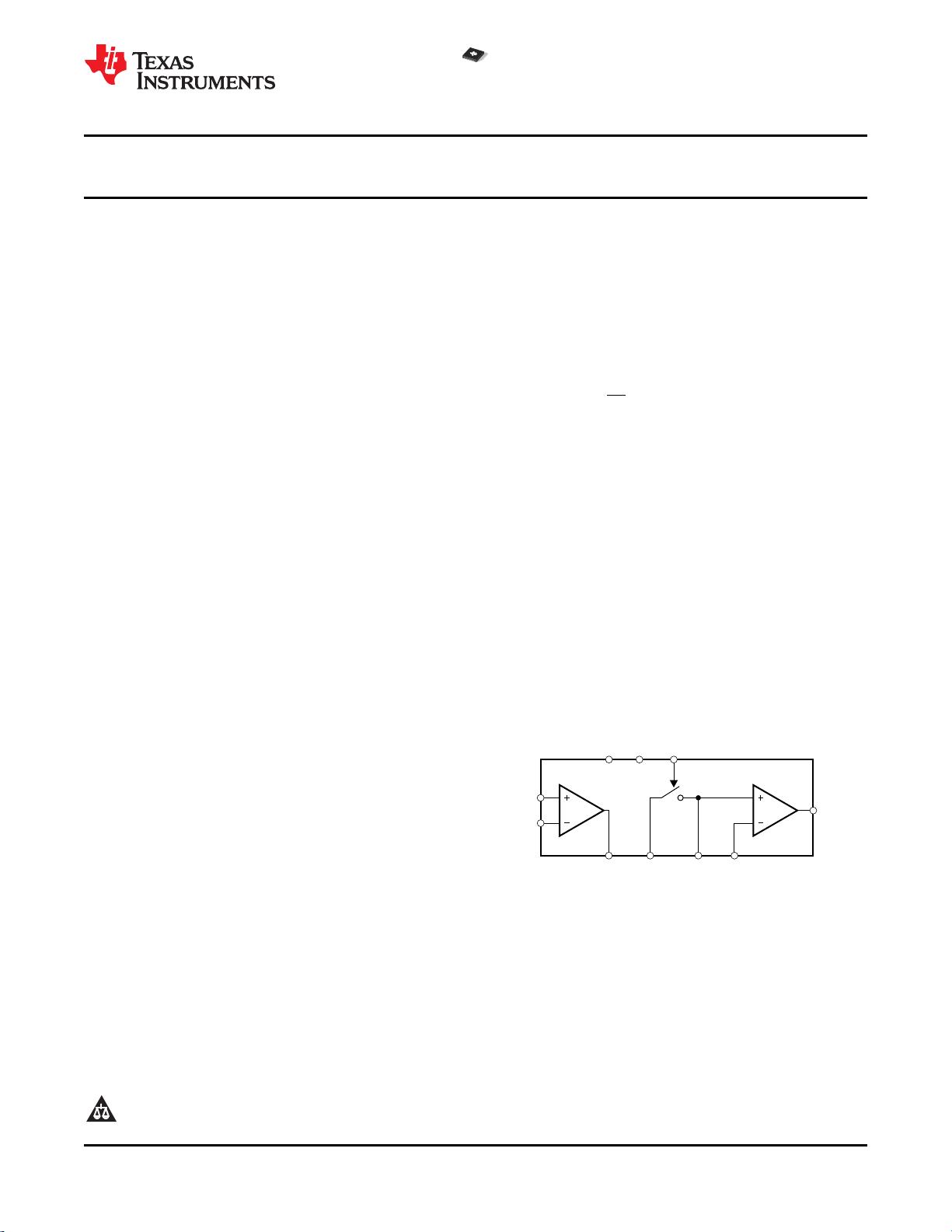
OPA1S2384 和 OPA1S2385 (OPA1S238x) 将高带
宽,场效应晶体管 (FET) 输入运算放大器与一个快速
• 高高转转换换率率::150V/μs
SPST COMS 开关组合在一起,设计用于需要跟踪和
• 轨轨到到轨轨输输入入/输输出出 (I/O)
捕捉快速信号的应用。
• 快快速速稳稳定定
• 低低输输入入偏偏置置电电流流::3pA
通过提供一个运行在单电源下的 250MHz 增益带宽产
• 高高输输入入阻阻抗抗::10
13
Ω || 2pF
品和轨到轨输入/输出开关,OPA1S238x 可同时实现
• SPST 开开关关::
宽带转阻增益和大输出信号摆幅。 低输入偏置电流和
– 低低导导通通电电阻阻::4Ω
电压噪声 (6nV/√Hz) 使得它可以放大极低电平的输入
– 低低电电荷荷注注入入::1pC
信号以实现最大的信噪比。
– 低低泄泄漏漏电电流流::10pA
OPA1S238x 的特点使得此器件非常适合被用作一个宽
• 灵灵活活配配置置::
带光二极管放大器。
– 转转阻阻增增益益
此外,CMOS 开关和其后的缓冲放大器使
– 外外部部保保持持电电容容
OPA1S238x 可被简单配置为一个快速采样保持电路。
– 后后级级增增益益
外部保持电容器和后级增益选项使得 OPA1S238x 可
• 单单电电源源::+2.7V 至至 +5.5V
轻松适应宽范围的速度和准确度要求。 请注
• 静静态态电电流流::9.2mA
意,OPA1S2384 使用一个逻辑高电平信号来关闭内部
• 小小型型封封装装::3mm x 3mm 小小外外形形尺尺寸寸无无引引线线
开关,而 OPA1S2385 使用一个低电平信号来关闭内
(SON)-10 封封装装
部开关。
• OPA1S2384::内内部部开开关关高高电电平平有有效效
• OPA1S2385::内内部部开开关关低低电电平平有有效效
OPA1S238x 针对低压运行(低至 +2.7V)到高达
+5.5V 电压运行进行了优化。这些器件的额定温度范围
应应用用范范围围
为 -40°C 至 +85°C。
• 通通信信::
– 光光网网络络::以以太太无无源源光光网网络络 (EPON),,千千兆兆无无源源光光
网网络络 (GPON)
– 信信号号强强度度监监视视器器
– 突突发发模模式式信信号号接接收收强强度度指指示示器器 (RSSI)
• 光光二二极极管管监监视视
• 快快速速采采样样保保持持电电路路
• 电电荷荷放放大大器器
(1) OPA1S2384 内部开关高电平有效;而
• 高高速速积积分分器器
OPA1S2385 内部开关低电平有效。
1
Please be aware that an important notice concerning availability, standard warranty, and use in critical applications of
Texas Instruments semiconductor products and disclaimers thereto appears at the end of this data sheet.
2All trademarks are the property of their respective owners.
PRODUCTION DATA information is current as of publication date.
Copyright © 2012–2013, Texas Instruments Incorporated
Products conform to specifications per the terms of the Texas
Instruments standard warranty. Production processing does not English Data Sheet: SBOS645
necessarily include testing of all parameters.

剩余23页未读,继续阅读
资源评论


