没有合适的资源?快使用搜索试试~ 我知道了~
TI-OPA3S2859.pdf
需积分: 9 0 下载量 61 浏览量
2022-11-26
21:42:10
上传
评论 4
收藏 2.28MB PDF 举报
温馨提示
试读
31页
TI-OPA3S2859.pdf
资源详情
资源评论
OPA3S2859 双通道 900 MHz、2.2 nV/√Hz 可编程增益跨阻放大器
1 特性
• 增益带宽积:900 MHz
• 内部可编程增益开关
• 高阻抗 FET 输入
• 输入电压噪声:2.2 nV/√Hz
• 压摆率:350 V/μs
• 电源电压范围:3.3V 至 5.25V
• 静态电流:22 mA/通道
• 断电模式 I
Q
:75 μA
• 温度范围:-40 °C 至 125 °C
2 应用
• 可切换的跨阻放大器
• 智能弹药
• 激光测距
• 光时域反射计 (OTDR)
• 硅光电倍增器 (SiPM) 缓冲放大器
• 光电倍增管后置放大器
• 高速可编程增益放大器
.
.
.
.
.
COM_A
FB_A2
FB_A1
FB_A0
INA+
100 k
10 k
1 k
VOUT_A
íVBIAS
íVBIAS
100 k
10 k
1 k
INB+
LTCH_B
LTCH_A
SEL0
VS-
VS+
PD
VS+
VS+
VS-
SEL1
INB-
COM_B
FB_B2
FB_B1
FB_B0
VOUT_B
+
±
+
±
INA-
1,0
0,0
0,1
0,1
0,0
1,0
方框图
3 说明
OPA3S2859 是一款具有 CMOS 输入的宽带低噪声可
编程增益放大器,适用于宽带跨阻和电压放大器应用。
当将该器件配置为跨阻放大器 (TIA) 时,0.9 GHz 增益
带宽积 (GBWP) 能够在低电容光电二极管 (PD) 应用中
实现高闭环带宽。
三个内部开关反馈路径以及一个可选的并行非开关反馈
路径最多允许四个可选增益配置。与使用分立式外部开
关的系统相比,内部开关将最大限度地降低寄生影响,
从而提高性能。每个开关针对 < 1 kΩ 到 > 100 kΩ 的
反馈电阻值进行了优化,适用于宽动态范围的应用。使
用两线制并行接口控制两个通道的选定开关路径。对于
所选的每个通道,也可以通过施加锁存引脚来使增益路
径保持恒定,这随后会禁用所选通道的开关控制,并防
止通道更改增益。
器件信息
(1)
器件型号 封装
封装尺寸(标称值)
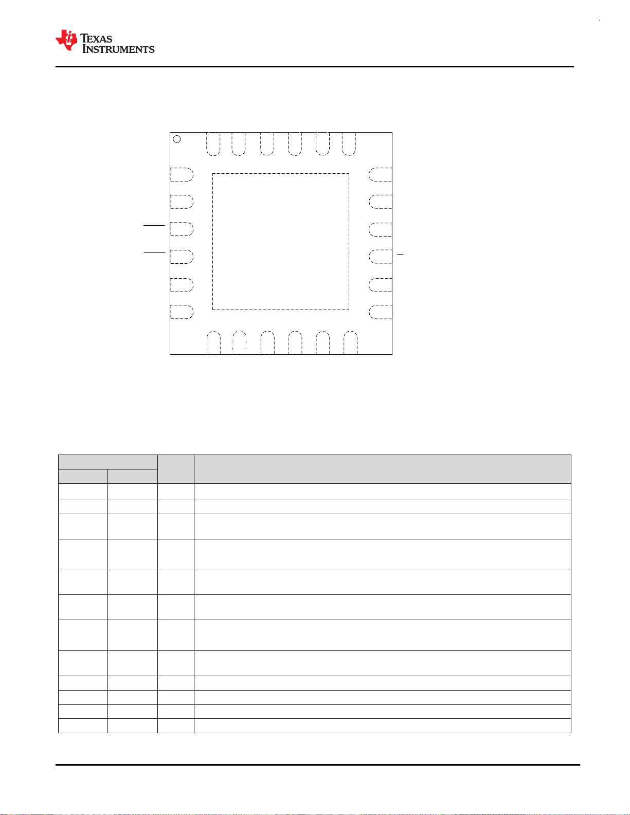
OPA3S2859 WQFN (24) 4.00mm × 4.00mm
(1) 如需了解所有可用封装,请参阅数据表末尾的封装选项附录。
.
.
.
Frequency (Hz)
Normalized Transimpedance (dB:)
-15
-12
-9
-6
-3
0
3
6
10M 100M 1G1M
OPA3
R
F
= 1 k:
R
F
= 10 k:
R
F
= 100 k:
跨阻带宽与频率间的关系
ADVANCE INFORMATION
OPA3S2859
ZHCSQB4 – MAY 2022
本文档旨在为方便起见,提供有关 TI 产品中文版本的信息,以确认产品的概要。有关适用的官方英文版本的最新信息,请访问
www.ti.com,其内容始终优先。TI 不保证翻译的准确性和有效性。在实际设计之前,请务必参考最新版本的英文版本。
English Data Sheet: SBOSA13
Table of Contents
1 特性................................................................................... 1
2 应用................................................................................... 1
3 说明................................................................................... 1
4 Revision History.............................................................. 2
5 Pin Configuration and Functions...................................3
6 Specifications.................................................................. 5
6.1 Absolute Maximum Ratings........................................ 5
6.2 ESD Ratings............................................................... 5
6.3 Recommended Operating Conditions.........................5
6.4 Thermal Information....................................................5
6.5 Electrical Characteristics.............................................6
6.6 Switching Characteristics............................................8
6.7 Typical Characteristics.............................................. 10
7 Parameter Measurement Information.......................... 16
8 Detailed Description......................................................17
8.1 Overview................................................................... 17
8.2 Functional Block Diagram......................................... 17
8.3 Feature Description...................................................18
8.4 Device Functional Modes..........................................18
9 Application and Implementation.................................. 20
9.1 Application Information............................................. 20
9.2 Typical Application.................................................... 20
10 Power Supply Recommendations..............................22
11 Layout........................................................................... 22
11.1 Layout Guidelines................................................... 22
11.2 Layout Examples.....................................................22
12 Device and Documentation Support..........................25
12.1 Device Support....................................................... 25
12.2 Documentation Support.......................................... 25
12.3 接收文档更新通知................................................... 25
12.4 支持资源..................................................................25
12.5 Trademarks.............................................................25
12.6 Electrostatic Discharge Caution..............................25
12.7 术语表..................................................................... 25
13 Mechanical, Packaging, and Orderable
Information.................................................................... 25
13.1 Tape and Reel Information......................................29
4 Revision History
DATE REVISION NOTES
May 2022 * Initial Release
OPA3S2859
ZHCSQB4 – MAY 2022
www.ti.com.cn
ADVANCE INFORMATION
2 Submit Document Feedback
Copyright © 2022 Texas Instruments Incorporated
Product Folder Links: OPA3S2859
5 Pin Configuration and Functions
1
21
20
19
22
INA+
6INB+
4
3
LTCH_B
LTCH_A
SEL0
5
23
VS-
PD
VS+
VS-
SEL1
2
INB-
8
9
FB_B2
10
FB_B1
11
FB_B0
12
VOUT_B
Thermal
Pad
VS+
COM_B
7
VOUT_A
FB_A1
FB_A0
COM_A
FB_A2
INA-
24
13
14
15
16
17
18
VS+
图 5-1. RTW Package,
24-Pin WQFN With Exposed Thermal Pad
(Top View)
表 5-1. Pin Functions
PIN
TYPE
(1)
DESCRIPTION
NAME NO.
COM_A 23 I
Photodiode input – Channel A
COM_B 8 I
Photodiode input – Channel B
FB_A0 20 I
Feedback connection to Channel A – TIA Gain Resistor (Low gain, optimized for gain in < 10 kΩ
range)
FB_A1 21 I
Feedback connection to Channel A – TIA Gain Resistor
(Mid gain, optimized for gain in 10 kΩ – 100 kΩ range)
FB_A2 22 I
Feedback connection to Channel A – TIA Gain Resistor (High gain, optimized for gain in > 100 kΩ
range)
FB_B0 11 I
Feedback connection to Channel B – TIA Gain Resistor (Low gain, optimized for gain in < 10 kΩ
range)
FB_B1 10 I
Feedback connection to Channel B – TIA Gain Resistor
(Mid gain, optimized for gain in 10 kΩ – 100 kΩ range)
FB_B2 9 I
Feedback connection to Channel B – TIA Gain Resistor (High gain, optimized for gain in > 100 kΩ
range)
INA- 24 I Negative (inverting) input for amplifier A
INA+ 1 I Positive (noninverting) input for amplifier A
INB- 7 I Negative (inverting) input for amplifier B
INB+ 6 I Positive (noninverting) input for amplifier B
www.ti.com.cn
OPA3S2859
ZHCSQB4 – MAY 2022
ADVANCE INFORMATION
Copyright © 2022 Texas Instruments Incorporated
Submit Document Feedback
3
Product Folder Links: OPA3S2859
表 5-1. Pin Functions (continued)
PIN
TYPE
(1)
DESCRIPTION
NAME NO.
LTCH_A 3 I
Latch control input for Channel A. LTCH_A = logic high (default) = transparent mode, gain setting
changes based on SEL0 and SEL1 pins are reflected at the output.
LTCH_A = logic low = latch mode = changing SEL0 and SEL1 pins does not affect the gain
configuration of amplifier.
LTCH_B 4 I
Latch control input for Channel B. LTCH_B = logic high (default) = transparent mode, gain setting
changes based on SEL0 and SEL1 pins are reflected at the output.
LTCH_B = logic low = latch mode = changing SEL0 and SEL1 pins does not affect the gain
configuration of amplifier.
PD 15 I Power down pin. PD = logic high (default) = normal operation, PD = logic low = power down mode.
SEL0 5 I
TIA gain selection. SEL0 = logic high (default). See 表 5-2 for details.
SEL1 2 I
TIA gain selection. SEL1 = logic high (default). See 表 5-2 for details.
VOUT_A 19 O Output of amplifier A
VOUT_B 12 O Output of amplifier B
VS- 13, 18 I Negative (lowest) power supply
VS+ 14, 16, 17 I Positive (highest) power supply
Thermal pad
—
Connect the thermal pad to the most negative power supply (pin 13 and 18) of the device under test
(DUT).
(1) I = input, O = output
表 5-2. Select Pin Decoder
SEL1 SEL0 Gain
LOW HIGH
Low Gain, optimized for gain in < 10 kΩ range
LOW LOW
Mid Gain, optimized for gain in 10 kΩ – 100 kΩ
range
HIGH LOW
High Gain, optimized for gain in > 100 kΩ range
HIGH (Default) HIGH (Default) External Gain. All internal switches open
OPA3S2859
ZHCSQB4 – MAY 2022
www.ti.com.cn
ADVANCE INFORMATION
4 Submit Document Feedback
Copyright © 2022 Texas Instruments Incorporated
Product Folder Links: OPA3S2859
6 Specifications
6.1 Absolute Maximum Ratings
over operating free-air temperature range (unless otherwise noted)
(1)
MIN MAX UNIT
V
S
Total supply voltage (V
S+
- V
S-
) 5.5 V
V
IN+
, V
IN-
Input voltage
(V
S–
) – 0.5
(V
S+
) + 0.5 V
V
ID
Differential input voltage 1 V
V
OUT
Output voltage
(V
S–
) – 0.5
(V
S+
) + 0.5 V
I
IN
Continuous input current ±4 mA
I
OUT
Continuous output current
(2)
25 mA
T
J
Junction temperature 150 °C
T
A
Operating free-air temperature
–40
125 °C
T
stg
Storage temperature
–65
150 °C
(1) Operation outside the Absolute Maximum Ratings may cause permanent device damage. Absolute maximum ratings do not imply
functional operation of the device at these or any other conditions beyond those listed under Recommended Operating Conditions. If
briefly operating outside the Recommended Operating Conditions but within the Absolute Maximum Ratings, the device may not
sustain damage, but it may not be fully functional. Operating the device in this manner may affect device reliability, functionality,
performance, and shorten the device lifetime.
(2) Long-term continuous output current for electromigration limits
6.2 ESD Ratings
VALUE UNIT
V
(ESD)
Electrostatic
discharge
Human body model (HBM), per ANSI/ESDA/JEDEC JS-001, all pins
(1)
±1500
V
Charged device model (CDM), per JEDEC specification JEDEC JS-002, all pins
(2)
±1000
(1) JEDEC document JEP155 states that 500-V HBM allows safe manufacturing with a standard ESD control process.
(2) JEDEC document JEP157 states that 250-V CDM allows safe manufacturing with a standard ESD control process.
6.3 Recommended Operating Conditions
over operating free-air temperature range (unless otherwise noted)
MIN NOM MAX UNIT
V
S
Total supply voltage (V
S+
- V
S-
) 3.3 5 5.25 V
T
A
Ambient temperature
–40
125 °C
6.4 Thermal Information
THERMAL METRIC
(1)
OPA3S2859
UNITRTW
24 PINS
R
θJA
Junction-to-ambient thermal resistance 52 °C/W
R
θJC(top)
Junction-to-case (top) thermal resistance 39.6 °C/W
R
θJB
Junction-to-board thermal resistance 28.2 °C/W
Ψ
JT
Junction-to-top characterization parameter 1.8 °C/W
Ψ
JB
Junction-to-board characterization parameter 28.2 °C/W
R
θJC(bot)
Junction-to-case (bottom) thermal resistance 13.3 °C/W
(1) For more information about traditional and new thermal metrics, see the Semiconductor and IC Package Thermal Metrics application
report.
www.ti.com.cn
OPA3S2859
ZHCSQB4 – MAY 2022
ADVANCE INFORMATION
Copyright © 2022 Texas Instruments Incorporated
Submit Document Feedback
5
Product Folder Links: OPA3S2859
剩余30页未读,继续阅读
安全验证
文档复制为VIP权益,开通VIP直接复制
信息提交成功
评论0
最新资源