没有合适的资源?快使用搜索试试~ 我知道了~
TI-TPS2411.pdf
需积分: 10 0 下载量 161 浏览量
2022-11-15
23:57:00
上传
评论 5
收藏 1.28MB PDF 举报
温馨提示
试读
31页
TI-TPS2411.pdf
资源详情
资源评论
UV
OV
V
DD
A
C
GND
GA TE
RSET
FL TR
R
(SET)
PG
FLTB
STAT
V ol tage Source
Note:ComponentsonRSET,FLTR,
UVandOVareOPTIONAL.
BY P
RSV D
Common V oltage Rail
A C
C
(BYP)
C
(FLTR)
Product
Folder
Order
Now
Technical
Documents
Tools &
Software
Support &
Community
本文档旨在为方便起见,提供有关 TI 产品中文版本的信息,以确认产品的概要。 有关适用的官方英文版本的最新信息,请访问 www.ti.com,其内容始终优先。 TI 不保证翻译的准确
性和有效性。 在实际设计之前,请务必参考最新版本的英文版本。
English Data Sheet: SLVS727
TPS2410
,
TPS2411
ZHCSK65E –NOVEMBER 2006–REVISED OCTOBER 2019
TPS241x 全全功功能能 N+1 和和 ORing 电电源源轨轨控控制制器器
1
1 特特性性
1
• 可控制用于 N+1 和 ORing 的外部 FET
• 3V 至 16.5V 的宽电源电压范围
• 控制总线电压范围为 0.8V 至 16.5V
• 线性或开/关控制方法
• 适用于 N 沟道 MOSFET 的内部电荷泵
• 快速器件关断功能可保护总线完整性
• 在热插入时进行主动栅极控制
• 软启动可降低总线瞬变
• 输入电压监控
• 短路栅极监控器
• MOSFET 控制状态指示灯
• 工业温度范围:–40°C 至 85°C
• 行业标准 14 引脚 TSSOP 封装
2 应应用用
• 机架式服务器(机架式)
• 机架式服务器(刀片式)
• 商用网络和服务器 PSU
• 电池备份单元
• 电信系统
3 说说明明
TPS241x 控制器与外部 N 沟道 MOSFET 配合使用,
可模拟低正向电压二极管的功能。该器件可以用于将多
电源与 N+1 配置中的公共总线相结合,或将冗余输入
电源总线进行结合。TPS2410 可提供线性启动控制功
能,而 TPS2411 具有开/关控制方法。
适用于 TPS2410x 的应用包括服务器和电信系统等各
种系统。这些 应用 通常具有 N+1 冗余电源或冗余电
源总线,或二者兼备。在故障和热插拔期间,这些冗余
电源必须具有等效二极管 OR 来防止产生反向电流。
相比于肖特基二极管,TPS241x 和 N 沟道 MOSFET
能够以更小的功率损耗提供此功能。
精确电压检测、可编程快速关断阈值和输入滤波允许根
据各种实施手段和总线特性量身定制运行方式。
提供了许多监控 功能 ,可用于指示电压总线
UV/OV、开/关状态和短路 MOSFET 栅极。
器器件件信信息息
(1)
器器件件型型号号 封封装装 封封装装尺尺寸寸((标标称称值值))
TPS2410
TPS2411
TSSOP (14) 5.00mm x 4.40mm
UQFN (14) 2.50mm x 2.50mm
(1) 如需了解所有可用封装,请参阅数据表末尾的可订购产品附
录。
典典型型应应用用图图
2
TPS2410
,
TPS2411
ZHCSK65E –NOVEMBER 2006–REVISED OCTOBER 2019
www.ti.com.cn
Copyright © 2006–2019, Texas Instruments Incorporated
目目录录
1 特特性性.......................................................................... 1
2 应应用用.......................................................................... 1
3 说说明明.......................................................................... 1
4 修修订订历历史史记记录录 ........................................................... 2
5 Device Comparison ............................................... 3
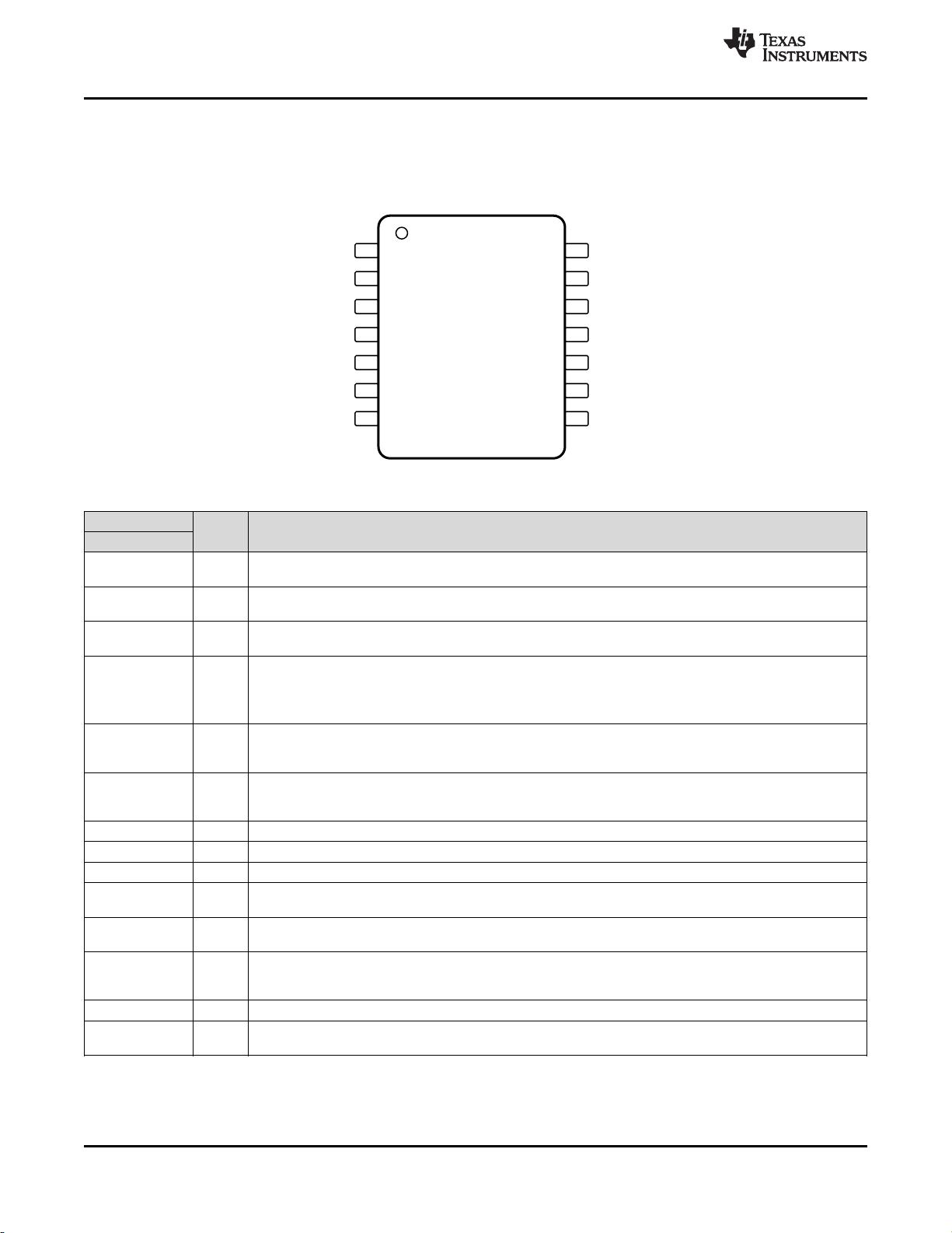
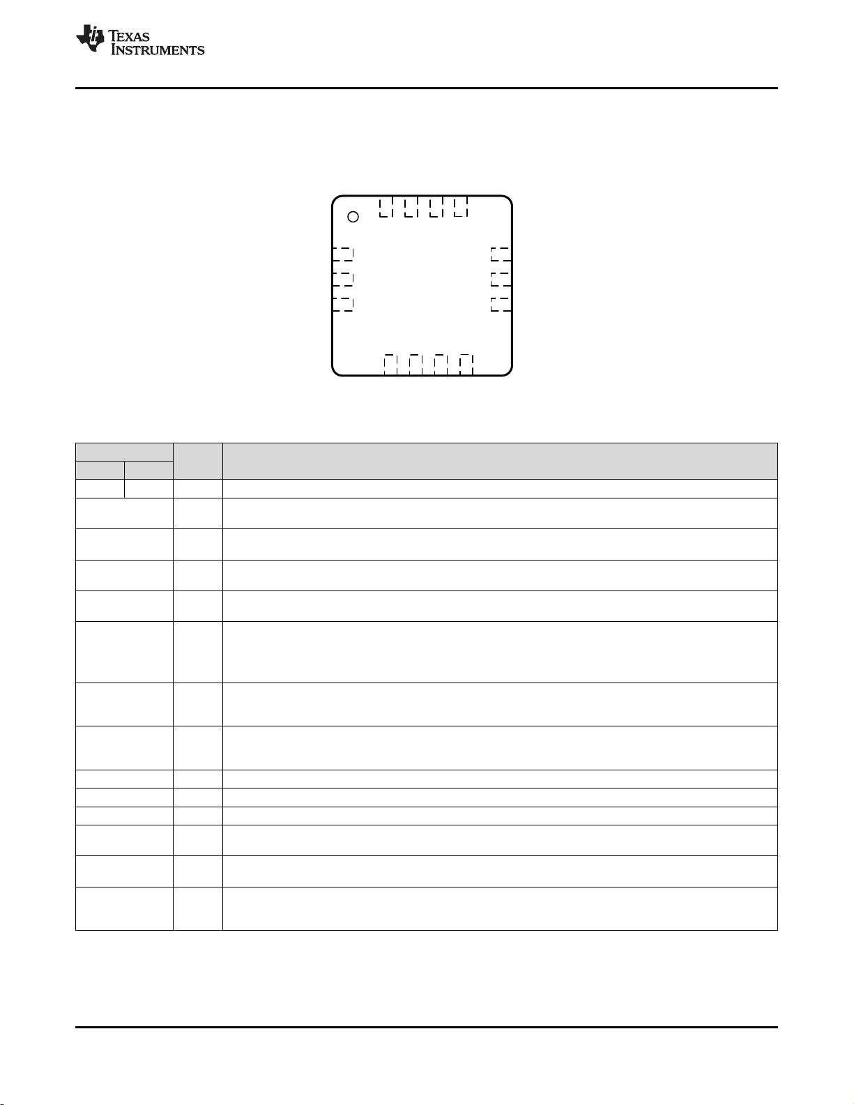
6 Pin Configuration and Functions......................... 4
7 Specifications......................................................... 6
7.1 Absolute Maximum Ratings ..................................... 6
7.2 ESD Ratings.............................................................. 6
7.3 Recommended Operating Conditions...................... 6
7.4 Thermal Information.................................................. 7
7.5 Electrical Characteristics: TPS2410, 11 ................... 7
7.6 Typical Characteristics.............................................. 9
8 Detailed Description............................................ 10
8.1 Overview ................................................................. 10
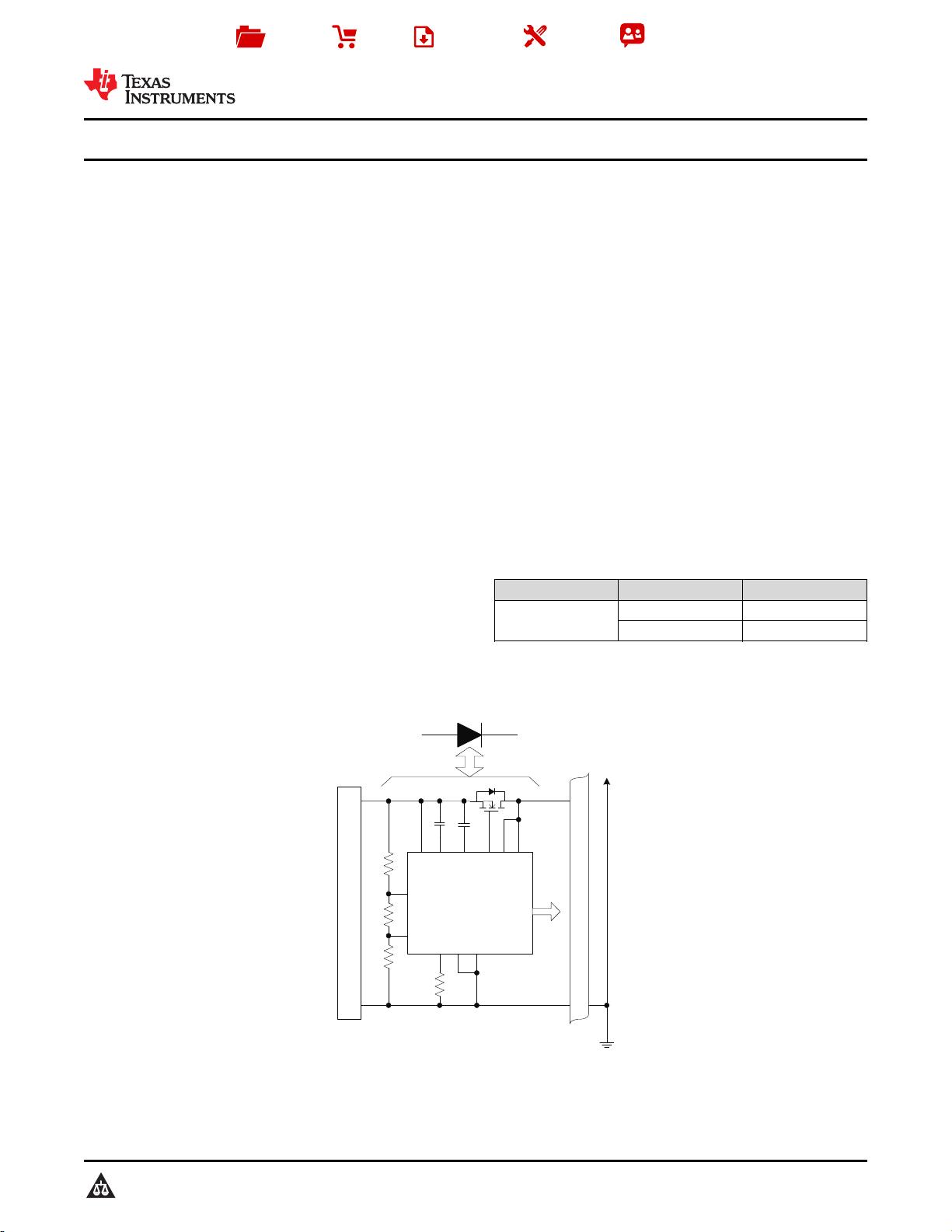
8.2 Functional Block Diagram ....................................... 10
8.3 Feature Description................................................. 10
8.4 Device Functional Modes........................................ 14
9 Application and Implementation ........................ 16
9.1 Typical Connections................................................ 16
9.2 Typical Application Examples ................................ 17
10 Power Supply Recommendations ..................... 23
10.1 Recommended Operating Range ......................... 23
10.2 System Design and Behavior with Transients ...... 23
11 Layout................................................................... 24
11.1 Layout Considerations .......................................... 24
11.2 Layout Example .................................................... 24
12 器器件件和和文文档档支支持持 ..................................................... 25
12.1 器件支持................................................................ 25
12.2 相关链接................................................................ 25
12.3 接收文档更新通知 ................................................. 25
12.4 社区资源................................................................ 25
12.5 商标 ....................................................................... 25
12.6 静电放电警告......................................................... 25
12.7 Glossary................................................................ 25
13 机机械械、、封封装装和和可可订订购购信信息息....................................... 25
4 修修订订历历史史记记录录
Changes from Revision D (August 2019) to Revision E Page
• Changed Gate positive drive MAX voltage from 11.5 to 12.5 in the Electrical Characteristics: TPS2410, 11
(2) (3) (4) (5)
(6) (7) (8)
table .......................................................................................................................................................................... 8
Changes from Revision C (June 2019) to Revision D Page
• 添加了
器件信息
表、ESD
额定值
表、
热性能信息
表、
特性 说明
部分、
器件功能模式
、
应用和实施
部分、
电源建议
部分、
布局
部分、
器件和文档支持
部分以及
机械、封装和可订购信息
部分 ......................................................................... 1
• 更改了
应用
列表...................................................................................................................................................................... 1
• Added the RMS (UQFN) pin configuration............................................................................................................................. 5
Changes from Revision B (November, 2006) to Revision C Page
• Changed I/O entry and description of STAT in the Pin Functions table................................................................................. 4
• Changed STAT pullup voltage in the Functional Block Diagram ......................................................................................... 10
• Changed STAT definition ..................................................................................................................................................... 12
• Changed figure to show STAT connection........................................................................................................................... 17
3
TPS2410
,
TPS2411
www.ti.com.cn
ZHCSK65E –NOVEMBER 2006–REVISED OCTOBER 2019
Copyright © 2006–2019, Texas Instruments Incorporated
5 Device Comparison
TPS2410 TPS2411 TPS2412 TPS2413
Linear gate control √ √
ON/OFF gate control √ √
Adjustable turn-off threshold √ √ √ √
Fast comparator filtering √ √
Voltage monitoring √ √
Enable control √ √
Mosfet fault monitoring √ √
Status pin √ √
1
V
DD
14 PG
2RS ET 13 BYP
3STAT 12 FL TR
4FL TB 11 A
5OV 10 C
6UV 9 RSVD
7GND 8 GATE
No t to scale
4
TPS2410
,
TPS2411
ZHCSK65E –NOVEMBER 2006–REVISED OCTOBER 2019
www.ti.com.cn
Copyright © 2006–2019, Texas Instruments Incorporated
6 Pin Configuration and Functions
PW Package
TSSOP 14 Pin
Top View
Pin Functions, PW
PIN
I/O DESCRIPTION
NAME NO.
V
DD
1 PWR
Input power for the gate drive charge pump and internal controls. V
DD
must be connected to a supply voltage
≥ 3 V.
RSET 2 I
Connect a resistor to ground to program the turn-off threshold. Leaving RSET open results in a slightly
positive V
(A-C)
turn-off threshold.
STAT 3 I/O
STAT is a multifunction pin. A high output indicates that the MOSFET gate is being driven high. Overdriving
STAT low while GATE is high shifts the fast-turnoff threshold negative. STAT has a weak pull-up to V
DD
.
FLTB 4 O
Open drain fault output. Fault is active (low) for any of the following conditions:
• Insufficient V
DD
• GATE should be high but is not.
• The MOSFET should be ON but the forward voltage exceeds 0.4 V.
OV 5 I
OV is a voltage monitor that contributes to the PG output, and also causes the MOSFET to turn off if it is
above the 0.6-V threshold. OV is programmable via an external resistor divider. An OV voltage above 0.6 V
indicates a bus voltage that is too high.
UV 6 I
UV is a voltage monitor that contributes to the PG output. The UV input has a 0.6 V threshold and is
programmable via an external resistor divider. A UV voltage above 0.6V indicates a bus voltage that is above
its minimum acceptable voltage. A low UV input does not effect the gate drive.
GND 7 PWR Device ground.
GATE 8 O Connect to the gate of the external MOSFET. Controls the MOSFET to emulate a low forward-voltage diode.
RSVD 9 PWR This pin must be connected to GND.
C 10 I
Voltage sense input that connects to the simulated diode cathode. Connect to the MOSFET drain in the
typical configuration.
A 11 I
Voltage sense input that connects to the simulated diode anode. A also serves as the reference for the
charge-pump bias supply on BYP. Connect to the MOSFET source in the typical configuration.
FLTR 12 I
A capacitor connected from FLTR to A filters the input to the fast comparator. Filtering allows the TPS2410 to
ignore spurious transients on the A and C inputs. This pin may be left open to achieve the fastest response
time.
BYP 13 I/O Connect a storage capacitor from BYP to A to filter the gate drive supply voltage.
PG 14 O
An open-drain Power Good indicator. PG is open if the UV input is above its threshold, the OV is below its
threshold, and the internal UVLO is satisfied.
14
4
1BYP 10 GATE
13
5
2PG 9 GND
6
3
V
DD
8 UV
No t to scale
12
11
7
FL TR
A
C
RS VD
RS ET
STAT
FL Tb
OV
5
TPS2410
,
TPS2411
www.ti.com.cn
ZHCSK65E –NOVEMBER 2006–REVISED OCTOBER 2019
Copyright © 2006–2019, Texas Instruments Incorporated
RMS Package
UQFN 14 Pin
Top View
Pin Functions, RMS
PIN
I/O DESCRIPTION
NAME NO.
BYP 1 I/O Connect a storage capacitor from BYP to A to filter the gate drive supply voltage.
PG; 2 O
An open-drain Power Good indicator. PG is open if the UV input is above its threshold, the OV is below its
threshold, and the internal UVLO is satisfied.
V
DD
3 PWR
Input power for the gate drive charge pump and internal controls. V
DD
must be connected to a supply voltage
≥ 3 V.
RSET 4 I
Connect a resistor to ground to program the turn-off threshold. Leaving RSET open results in a slightly
positive V
(A-C)
turn-off threshold.
STAT 5 I/O
STAT is a multifunction pin. A high output indicates that the MOSFET gate is being driven high. Overdriving
STAT low while GATE is high shifts the fast-turnoff threshold negative. STAT has a weak pull-up to V
DD
.
FLTB 6 O
Open drain fault output. Fault is active (low) for any of the following conditions:
• Insufficient V
DD
• GATE should be high but is not.
• The MOSFET should be ON but the forward voltage exceeds 0.4 V.
OV 7 I
OV is a voltage monitor that contributes to the PG output, and also causes the MOSFET to turn off if it is
above the 0.6-V threshold. OV is programmable via an external resistor divider. An OV voltage above 0.6 V
indicates a bus voltage that is too high.
UV 8 I
UV is a voltage monitor that contributes to the PG output. The UV input has a 0.6 V threshold and is
programmable via an external resistor divider. A UV voltage above 0.6V indicates a bus voltage that is above
its minimum acceptable voltage. A low UV input does not effect the gate drive.
GND 9 PWR Device ground.
GATE 10 O Connect to the gate of the external MOSFET. Controls the MOSFET to emulate a low forward-voltage diode.
RSVD 11 PWR This pin must be connected to GND.
C 12 I
Voltage sense input that connects to the simulated diode cathode. Connect to the MOSFET drain in the
typical configuration.
A 13 I
Voltage sense input that connects to the simulated diode anode. A also serves as the reference for the
charge-pump bias supply on BYP. Connect to the MOSFET source in the typical configuration.
FLTR 14 I
A capacitor connected from FLTR to A filters the input to the fast comparator. Filtering allows the TPS2410 to
ignore spurious transients on the A and C inputs. This pin may be left open to achieve the fastest response
time.
剩余30页未读,继续阅读
安全验证
文档复制为VIP权益,开通VIP直接复制
信息提交成功
评论0
最新资源