TI-TPS2483.pdf
需积分: 10 137 浏览量
2022-11-15
23:47:23
上传
评论 5
收藏 2.21MB PDF 举报

TPS2482
TPS2483
www.ti.com.cn
ZHCSAJ1A –DECEMBER 2012–REVISED MARCH 2013
具具有有精精准准 I
2
C 功功率率监监控控的的 36V 热热插插拔拔控控制制器器
查查询询样样品品: TPS2482, TPS2483
1
特特性性
说说明明
2
• 输输入入电电压压范范围围为为 9V 至至 36V,,绝绝对对最最大大值值 40V
TPS2482 和 TPS2483 提供针对 9V 至 36V 应用的热
插拔控制和精准监控。 精确电压、电流和功率监控由
• 电电流流、、电电压压和和功功率率监监控控
16 位模数 (A/D) 转换器,此转换器具有一个与 I
2
C 和
• ±0.5% 准准确确电电流流监监控控
(-25°C<T
J
<85°C)
SMBus 兼容的串行接口。 电压和电流测量内部交叉且
• 16 个个可可编编程程 I
2
C™ 地地址址
被复合在一起以提供并发功率计算。 这些器件在温度
• 可可配配置置取取平平均均选选项项
和宽负载范围内具有高电流监控精度。 这使得它们非
• 可可编编程程金金属属氧氧化化物物半半导导体体场场效效应应晶晶体体管管 (MOSFET)
常适合于负载特性和健康运行由电流配置确定的应用,
SOA 保保护护
诸如远程射频头或蜂窝天线应用。
• 针针对对外外部部 N-FET 的的高高侧侧栅栅极极驱驱动动
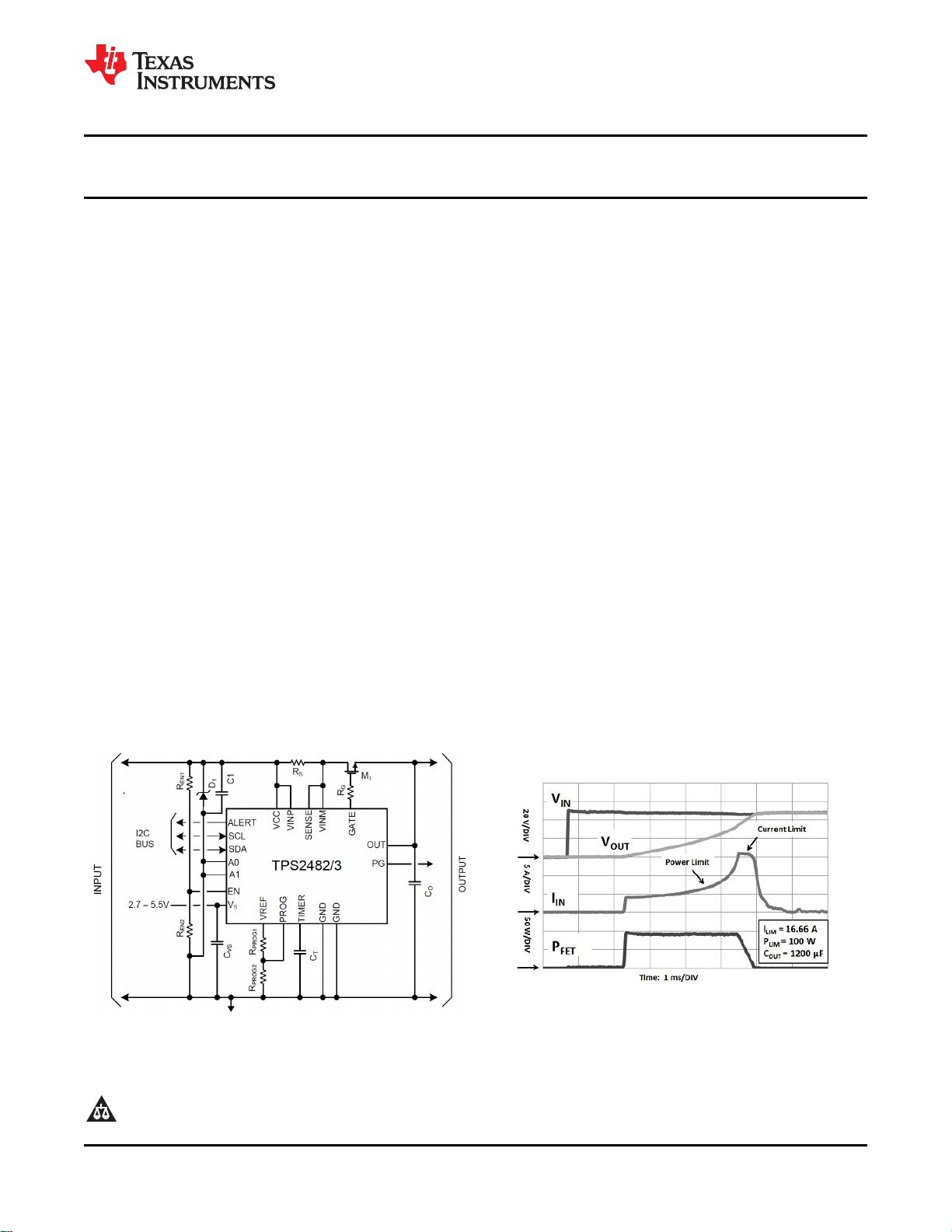
热插拔部分驱动 N 通道 MOSFET,此 MOSFET 具有
• 可可编编程程故故障障定定时时器器
同步涌入和故障电流限制功能。 先进的 MOSFET 安
• 开开漏漏电电源源正正常常输输出出
全运行区域 (SOA) 保护由可编程恒定功率折返和固定
• 20 引引脚脚薄薄型型小小外外形形尺尺寸寸 (TSSOP) 封封装装
电流限制来实现。 这引起了如下面的启动图表中显示
的一个指数涌入电流概图。 由于 V
OUT
斜升,而
应应用用范范围围
MOSFET 的 V
DS
被减少,电流的增加一直将 MOSFET
• RRH((远远程程射射频频头头))
功率耗散保持在其 SOA 范围内。 TPS2482 在一个硬
• 存存储储网网络络
件故障后锁存,而 TPS2483 在冷关机延迟后自动尝试
• 插插件件模模块块
重新启动。
• 基基站站 24V 天天线线电电源源
TPS2482 和 TPS2483 可被插入现有的 TPS2480 和
• 工工业业用用 24V - 28V 电电源源
TPS2481 插座内来提升精度和运行电压范围。 无需进
行印刷电路板 (PCB) 更改和只需微小的软件修改即可
实现。
简简化化的的应应用用示示意意图图
示示例例启启动动波波形形
1
Please be aware that an important notice concerning availability, standard warranty, and use in critical applications of
Texas Instruments semiconductor products and disclaimers thereto appears at the end of this data sheet.
2I
2
C is a trademark of NXP B.V Corporation.
PRODUCTION DATA information is current as of publication date.
版权 © 2012–2013, Texas Instruments Incorporated
Products conform to specifications per the terms of the Texas
Instruments standard warranty. Production processing does not English Data Sheet: SLUSAW1
necessarily include testing of all parameters.
剩余55页未读,继续阅读


评论0
最新资源