没有合适的资源?快使用搜索试试~ 我知道了~
TI-TPS2202A.pdf
需积分: 10 0 下载量 98 浏览量
2022-11-14
23:04:48
上传
评论 5
收藏 326KB PDF 举报
温馨提示
试读
23页
TI-TPS2202A.pdf
资源推荐
资源详情
资源评论
TPS2202AI
DUAL-SLOT PC CARD POWER-INTERFACE SWITCH
WITH RESET FOR SERIAL PCMCIA CONTROLLER
SLVS123B – SEPTEMBER 1995 – REVISED JANUARY 2001
1
POST OFFICE BOX 655303 • DALLAS, TEXAS 75265
D
Fully Integrated V
CC
and V
pp
Switching for
Dual-Slot PC Card Interface
D
P
2
C 3-Lead Serial Interface Compatible
With CardBus Controllers
D
Meets PC Card Standards
D
RESET Allows System Initialization of PC
Cards
D
12-V Supply Can Be Disabled Except
During 12-V Flash Programming
D
Short-Circuit and Thermal Protection
D
Space-Saving 30-Pin SSOP (DB) Package
D
Compatible With 3.3-V, 5-V and 12-V PC
Cards
D
Power Saving I
DD
= 83 µA Typ, I
Q
= 1 µA
D
Low r
DS(on)
(160-mΩ V
CC
Switch)
D
Break-Before-Make Switching
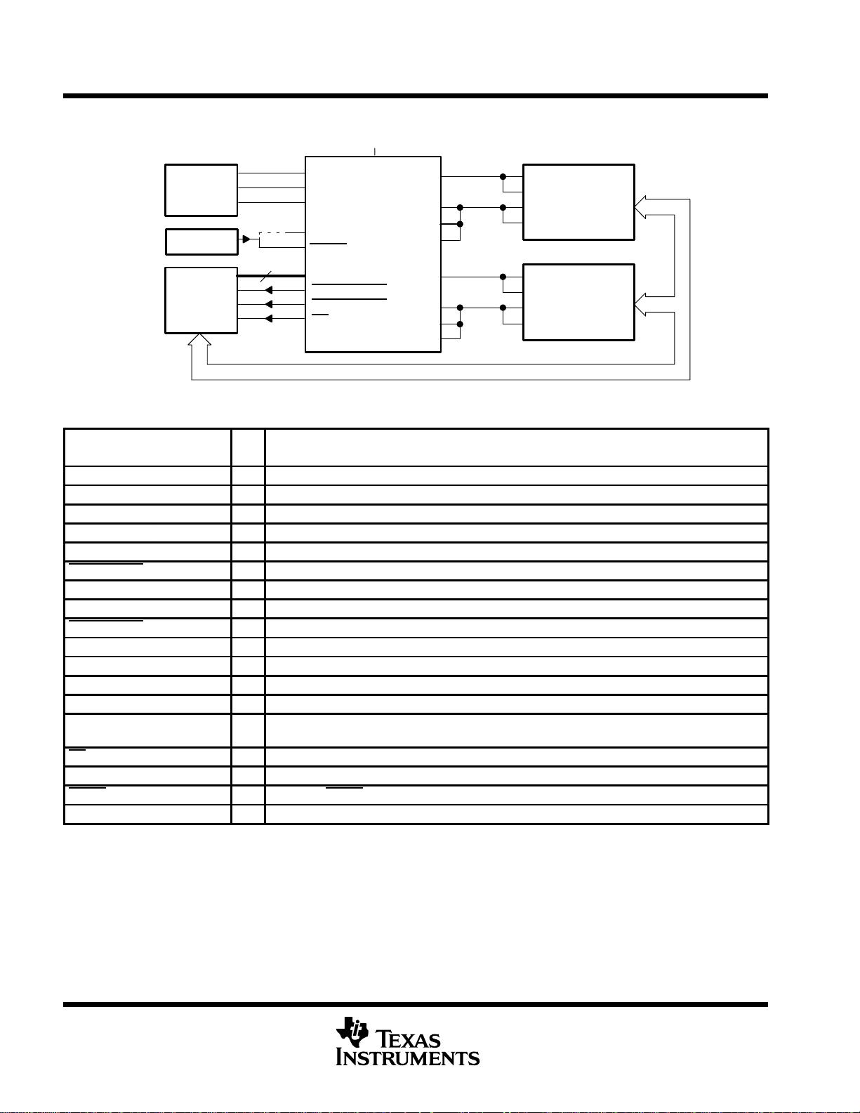
description
The TPS2202AI PC Card power-interface switch provides an integrated power-management solution for two
PC Cards. All of the discrete power MOSFETs, a logic section, current limiting, thermal protection, and
power-good reporting for PC Card control are combined on a single integrated circuit (IC), using the Texas
Instruments LinBiCMOS process. The circuit allows the distribution of 3.3-V, 5-V, and/or 12-V card power by
means of the P
2
C (PCMCIA Peripheral-Control) Texas Instruments nonproprietary serial interface. The
current-limiting feature eliminates the need for fuses, which reduces component count and improves reliability.
Current-limit reporting can help the user isolate a system fault to a specific card.
The TPS2202AI incorporates a reset function, selectable by one of two inputs, to help alleviate system errors.
The reset function enables PC Card initialization concurrent with host platform initialization, allowing a system
reset. Reset is accomplished by grounding the V
CC
and V
pp
(flash-memory programming voltage) outputs,
which discharges residual card voltage.
End equipment for the TPS2202AI includes notebook computers, desktop computers, personal digital assistants
(PDAs), digital cameras, handiterminals, and bar-code scanners.
AVAILABLE OPTIONS
PACKAGED DEVICES
T
J
SSOP
(DB)
†
SSOP
(DF)
†
–40°C to 150°C TPS2202AIDBR TPS2202AIDFR
†
The DB and DF packages are only available taped and reeled,
inidcated by the R suffix on the device type.
LinBiCMOS and P
2
C are trademarks of Texas Instruments.
PC Card and CardBus are trademarks of PCMCIA (Personal Computer Memory Card International Association).
Copyright 2001, Texas Instruments Incorporated
PRODUCTION DATA information is current as of publication date.
Products conform to specifications per the terms of Texas Instruments
standard warranty. Production processing does not necessarily include
testing of all parameters.
Please be aware that an important notice concerning availability, standard warranty, and use in critical applications of
Texas Instruments semiconductor products and disclaimers thereto appears at the end of this data sheet.
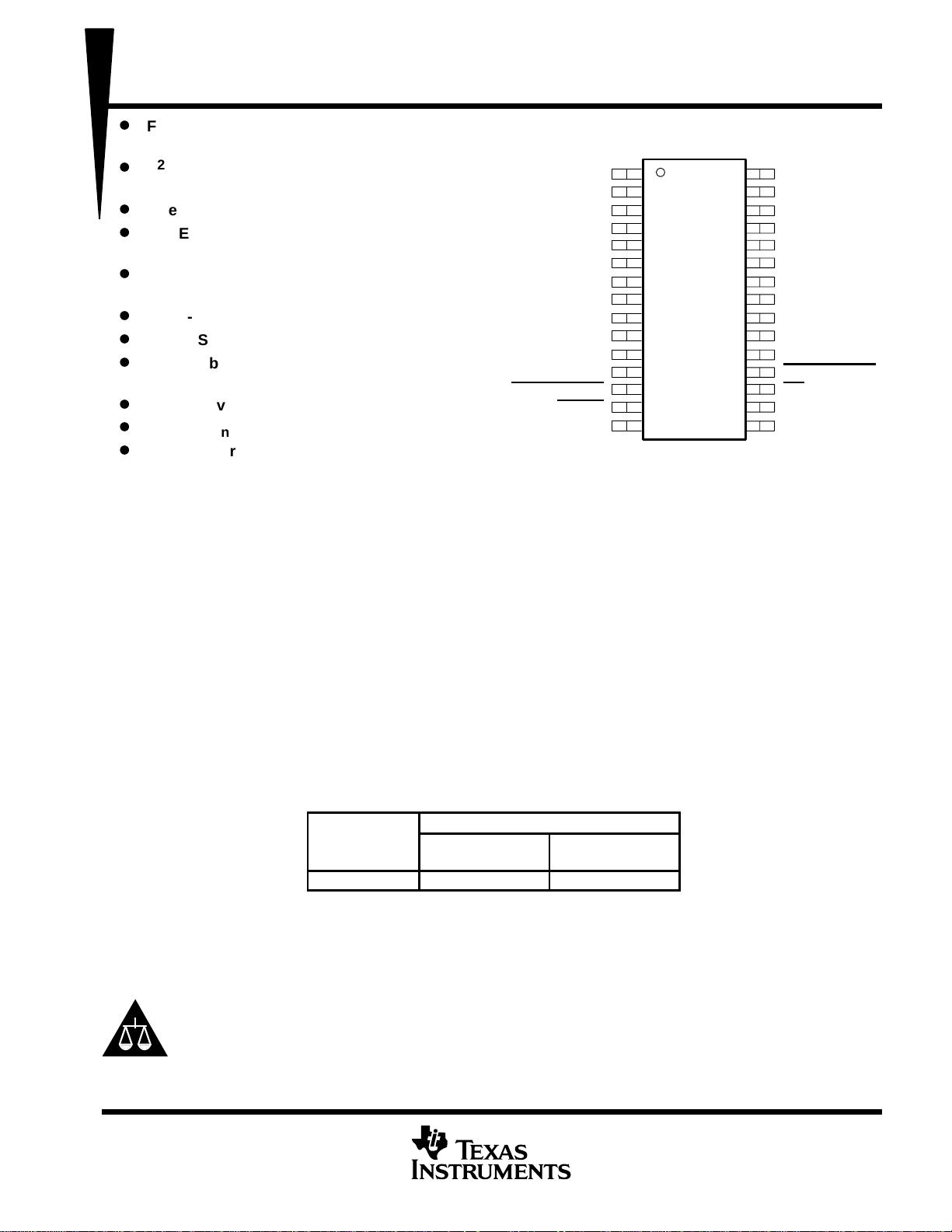
1
2
3
4
5
6
7
8
9
10
11
12
13
14
15
30
29
28
27
26
25
24
23
22
21
20
19
18
17
16
5V
5V
DATA
CLOCK
LATCH
RESET
12V
AVPP
AVCC
AVCC
AVCC
GND
APWR_GOOD
RESET
3.3V
5V
NC
NC
NC
NC
V
DD
12V
BVPP
BVCC
BVCC
BVCC
BPWR_GOOD
OC
3.3V
3.3V
DB OR DF PACKAGE
(TOP VIEW)
NC – No internal connection
TPS2202AI
DUAL-SLOT PC CARD POWER-INTERFACE SWITCH
WITH RESET FOR SERIAL PCMCIA CONTROLLER
SLVS123B – SEPTEMBER 1995 – REVISED JANUARY 2001
2
POST OFFICE BOX 655303 • DALLAS, TEXAS 75265
typical PC card power-distribution application
PCMCIA
Controller
12 V
Power Supply
V
pp1
V
pp2
V
CC
V
CC
PC
Card A
V
DD
TPS2202AI
5 V
3.3 V
BPWR_GOOD
OC
Serial Interface
3
V
pp1
V
pp2
V
CC
V
CC
PC
Card B
12V
5V
3.3V
AVPP
AVCC
AVCC
BVPP
BVCC
BVCC
APWR_GOOD
BVCC
AVCC
Supervisor
RESET
RESET
Terminal Functions
TERMINAL
I/O
DESCRIPTION
NAME NO.
I/O
DESCRIPTION
3.3V 15, 16, 17 I 3.3-V V
CC
input for card power
5V 1, 2, 30 I 5-V V
CC
input for card power
12V 7, 24 I 12-V V
pp
input for card power
AVCC 9, 10, 11 O Switched output that delivers 3.3 V, 5 V, low or high impedance to card
AVPP 8 O Switched output that delivers 3.3 V, 5 V, 12 V, low or high impedance to card
APWR_GOOD 13 O Logic-level power-ready output that stays low as long as AVPP is within limits
BVCC 20, 21, 22 O Switched output that delivers 3.3 V, 5 V, low or high impedance
BVPP 23 O Switched output that delivers 3.3 V, 5 V, 12 V, low or high impedance
BPWR_GOOD 19 O Logic-level power-ready output that remains low as long as BVPP is within limits
CLOCK 4 I Logic-level clock for serial data word
DATA 3 I Logic-level serial data word
GND 12 Ground
LATCH 5 I Logic-level latch for serial data word
NC 26, 27,
28, 29
No internal connection
OC 18 O Logic-level overcurrent reporting output that goes low when an overcurrent condition exists
RESET 6 I Logic-level RESET input active high. Do not connect if terminal 14 is used.
RESET 14 I Logic-level RESET input active low. Do not connect if terminal 6 is used.
V
DD
25 I 5-V power to chip
TPS2202AI
DUAL-SLOT PC CARD POWER-INTERFACE SWITCH
WITH RESET FOR SERIAL PCMCIA CONTROLLER
SLVS123B – SEPTEMBER 1995 – REVISED JANUARY 2001
3
POST OFFICE BOX 655303 • DALLAS, TEXAS 75265
absolute maximum ratings over operating free-air temperature (unless otherwise noted)
†
Supply voltage range, V
DD
–0.3 V to 7 V. . . . . . . . . . . . . . . . . . . . . . . . . . . . . . . . . . . . . . . . . . . . . . . . . . . . . . . . . .
Input voltage range for card power: V
I(5V)
–0.3 V to 7 V. . . . . . . . . . . . . . . . . . . . . . . . . . . . . . . . . . . . . . . . . . . . .
V
I(3.3V)
–0.3 V to V
I(5V)
. . . . . . . . . . . . . . . . . . . . . . . . . . . . . . . . . . . . . . . . .
V
I(12V)
–0.3 V to 14 V. . . . . . . . . . . . . . . . . . . . . . . . . . . . . . . . . . . . . . . . . . .
Logic input voltage –0.3 V to 7 V. . . . . . . . . . . . . . . . . . . . . . . . . . . . . . . . . . . . . . . . . . . . . . . . . . . . . . . . . . . . . . . . .
Continuous total power dissipation See Dissipation Rating Table. . . . . . . . . . . . . . . . . . . . . . . . . . . . . . . . . . . . .
Output current (each card): I
O(xVCC)
internally limited. . . . . . . . . . . . . . . . . . . . . . . . . . . . . . . . . . . . . . . . . . . . . .
I
O(xVPP)
internally limited. . . . . . . . . . . . . . . . . . . . . . . . . . . . . . . . . . . . . . . . . . . . . .
Operating virtual junction temperature range, T
J
–40°C to 150°C. . . . . . . . . . . . . . . . . . . . . . . . . . . . . . . . . . . . .
Operating free-air temperature range, T
A
–40°C to 85°C. . . . . . . . . . . . . . . . . . . . . . . . . . . . . . . . . . . . . . . . . . . .
Storage temperature range, T
stg
–55°C to 150°C. . . . . . . . . . . . . . . . . . . . . . . . . . . . . . . . . . . . . . . . . . . . . . . . . . .
Lead temperature 1,6 mm (1/16 inch) from case for 10 seconds 260°C. . . . . . . . . . . . . . . . . . . . . . . . . . . . . . .
†
Stresses beyond those listed under “absolute maximum ratings” may cause permanent damage to the device. These are stress ratings only, and
functional operation of the device at these or any other conditions beyond those indicated under “recommended operating conditions” is not
implied. Exposure to absolute-maximum-rated conditions for extended periods may affect device reliability.
DISSIPATION RATING TABLE
PACKAGE
T
A
≤ 25°C
POWER RATING
DERATING FACTOR
‡
ABOVE T
A
= 25°C
T
A
= 70°C
POWER RATING
T
A
= 85°C
POWER RATING
DF 1158 mW 9.26 mW/°C 741 mW 602 mW
DB 1024 mW 8.2 mW/°C 655 mW 532 mW
‡
These devices are mounted on an FR4 board with no special thermal considerations.
recommended operating conditions
MIN MAX UNIT
Supply voltage, V
DD
4.75 5.25 V
V
I(5V)
0 5.25 V
Input voltage range, V
I
V
I(3.3V)
0 V
I(5V)
§
V
V
I(12V)
0 13.5 V
Out
p
ut current
I
O(xVCC)
at 25°C 1 A
Output
current
I
O(xVPP)
at 25°C 150 mA
Clock frequency 0 2.5 MHz
Operating virtual junction temperature, T
J
–40 125 °C
§
V
I(3.3V)
should not be taken above V
I(5V)
.
TPS2202AI
DUAL-SLOT PC CARD POWER-INTERFACE SWITCH
WITH RESET FOR SERIAL PCMCIA CONTROLLER
SLVS123B – SEPTEMBER 1995 – REVISED JANUARY 2001
4
POST OFFICE BOX 655303 • DALLAS, TEXAS 75265
electrical characteristics, T
A
= 25°C, V
DD
= 5 V (unless otherwise noted)
dc characteristics
PARAMETER TEST CONDITIONS MIN TYP MAX UNIT
†
5 V to xVCC 160
mΩ
†
3.3 V to xVCC 225
mΩ
Switch resistances
†
5 V to xVPP 6
3.3 V to xVPP 6
Ω
12 V to xVPP 1
V
O(xVPP)
Clamp low voltage I
pp
at 10 mA 0.8 V
V
O(xVCC)
Clamp low voltage I
CC
at 10 mA 0.8 V
I
pp
Hi
g
h-impedance
T
A
= 25°C 1 10
I
lk
Leakage current
g
state
T
A
= 85°C 50
µA
I
lkg
Leakage
current
I
CC
Hi
g
h-impedance
T
A
= 25°C 1 10
µ
A
CC
g
state
T
A
= 85°C 50
I
I
In
p
ut current
I
DD
Supply current
V
O(AVCC)
= V
O(BVCC)
= 5 V,
V
O(AVPP)
= V
O(BVPP)
= 12 V
83 150 µA
I
I
Input
current
I
DD
Supply current
in shutdown
V
O(BVCC)
= V
O(AVCC)
= V
O(AVPP)
= V
O(BVPP)
= Hi-Z
1 µA
Power-ready threshold,
PWR_GOOD
10.72 11.05 11.4 V
Power-ready hysteresis,
PWR_GOOD
12-V mode 50 mV
Short-circuit output-
I
O(xVCC)
T
J
= 85°C,
0.75 1.3 1.9 A
current limit
I
O(xVPP)
J
,
Output powered up into a short to GND
120 200 400 mA
†
Pulse-testing techniques are used to maintain junction temperature close to ambient temperature; thermal effects must be taken into account
separately.
logic section
PARAMETER TEST CONDITIONS MIN MAX UNIT
Logic input current 1 µA
Logic input high level 2 V
Logic input low level 0.8 V
Logic output high level
I
O
=1mA
V
DD
–0.4 V
Logic output low level
I
O
=
1
mA
0.4 V
Logic input minimum pulse width 1 µs
TPS2202AI
DUAL-SLOT PC CARD POWER-INTERFACE SWITCH
WITH RESET FOR SERIAL PCMCIA CONTROLLER
SLVS123B – SEPTEMBER 1995 – REVISED JANUARY 2001
5
POST OFFICE BOX 655303 • DALLAS, TEXAS 75265
switching characteristics
†
PARAMETER TEST CONDITIONS MIN TYP MAX UNIT
t Out
p
ut rise times
V
O(xVCC)
1.2
t
r
Output
rise
times
V
O(xVPP)
5
ms
t
f
Out
p
ut fall times
V
O(xVCC)
10
ms
t
f
Output
fall
times
V
O(xVPP)
14
‡
LATCH↑ to V
O( )
t
on
5.8 ms
‡
LATCH↑
t
o
V
O(xVPP)
t
off
18 ms
t
d
Pro
p
agation delay (see Figure 1
‡
)
LATCH↑ to xVCC (3 V)
t
on
5.8 ms
t
pd
Propagation
delay
(see
Figure
1
‡
)
LATCH↑
t
o x
VCC
(3
V)
t
off
28 ms
LATCH↑ to xVCC (5 V)
t
on
4 ms
LATCH↑
to
xVCC
(5
V)
t
off
30 ms
†
Refer to Parameter Measurement Information
‡
Propagation delays are with C
L
= 100 µF.
剩余22页未读,继续阅读
资源评论
不觉明了
- 粉丝: 3103
- 资源: 5348
上传资源 快速赚钱
- 我的内容管理 展开
- 我的资源 快来上传第一个资源
- 我的收益 登录查看自己的收益
- 我的积分 登录查看自己的积分
- 我的C币 登录后查看C币余额
- 我的收藏
- 我的下载
- 下载帮助
安全验证
文档复制为VIP权益,开通VIP直接复制
信息提交成功