没有合适的资源?快使用搜索试试~ 我知道了~
TI-LM137HVQML.pdf
需积分: 9 0 下载量 167 浏览量
2022-10-28
21:20:45
上传
评论 5
收藏 682KB PDF 举报
温馨提示
试读
15页
TI-LM137HVQML.pdf
资源推荐
资源详情
资源评论
LM137HVQML
www.ti.com
SNVS314A –DECEMBER 2010–REVISED APRIL 2013
LM137HVQML 3-Terminal Adjustable Negative Regulators (High Voltage)
Check for Samples: LM137HVQML
1
FEATURES
DESCRIPTION
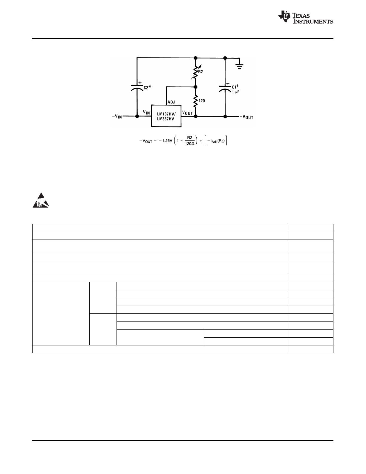
The LM137HV is an adjustable 3-terminal negative
2
• Output Voltage Adjustable from −47V to −1.2V
voltage regulator capable of supplying in excess of
• 1.5A Output Current Specified, −55°C ≤ T
J
≤
−1.5A over an output voltage range of −47V to −1.2V.
+150°C
This regulators is exceptionally easy to apply,
• Line Regulation Typically 0.01%/V
requiring only 2 external resistors to set the output
voltage and 1 output capacitor for frequency
• Load Regulation Typically 0.3%
compensation. The circuit design has been optimized
• Excellent Thermal Regulation, 0.002%/W
for excellent regulation and low thermal transients.
• 77 dB Ripple Rejection
Further, the LM137HV features internal current
limiting, thermal shutdown and safe-area
• Excellent Rejection of Thermal Transients
compensation, making them virtually blowout-proof
• 50 ppm/°C Temperature Coefficient
against overloads.
• Temperature-Independent Current Limit
The LM137HV serves a wide variety of applications
• Internal Thermal Overload Protection
including local on-card regulation, programmable-
• Standard 3-Lead Transistor Package
output voltage regulation or precision current
regulation. The LM137HV is an ideal complement to
• Output Short Circuit Protected
the LM117HV adjustable positive regulator.
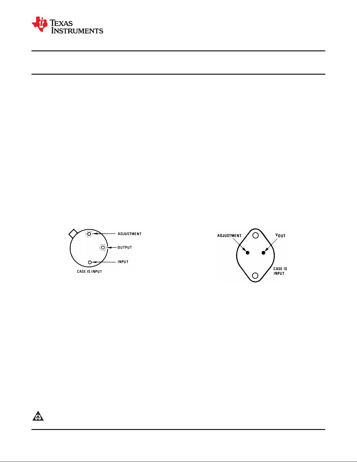
Connection Diagrams
See Physical Dimensions section for further information
Figure 1. TO Package – Bottom View Figure 2. TO-3 Package (Bottom View)
See Package Number NDT0003A See Package Number K
1
Please be aware that an important notice concerning availability, standard warranty, and use in critical applications of
Texas Instruments semiconductor products and disclaimers thereto appears at the end of this data sheet.
2All trademarks are the property of their respective owners.
PRODUCTION DATA information is current as of publication date.
Copyright © 2010–2013, Texas Instruments Incorporated
Products conform to specifications per the terms of the Texas
Instruments standard warranty. Production processing does not
necessarily include testing of all parameters.
LM137HVQML
SNVS314A –DECEMBER 2010–REVISED APRIL 2013
www.ti.com
Typical Applications
†
C1 = 1 μF solid tantalum or 10 μF aluminum electrolytic required for stability. Output capacitors in the range of 1 μF
to 1000 μF of aluminum or tantalum electrolytic are commonly used to provide improved output impedance and
rejection of transients.
*
C2 = 1 μF solid tantalum is required only if regulator is more than 4″ from power-supply filter capacitor.
Figure 3. Adjustable Negative Voltage Regulator
These devices have limited built-in ESD protection. The leads should be shorted together or the device placed in conductive foam
during storage or handling to prevent electrostatic damage to the MOS gates.
Absolute Maximum Ratings
(1)
Power Dissipation
(2)
Internally limited
Input—Output Voltage Differential 50V
Operating Ambient Temperature Range −55°C ≤ T
A
≤
+125°C
Maximum Junction Temperature Range +150°C
Storage Temperature −65°C ≤ T
A
≤
+150°C
Lead Temperature (Soldering, 10 sec.) 300°C
Thermal Resistance θ
JA
NDT0003A pkg. (Still Air @ 0.5W) 174°C/W
NDT0003A pkg. (500LF / Min Air Flow @ 0.5W) 64°C/W
K pkg. (Still Air @ 0.5W) 42°C/W
K pkg. (500LF / Min Air Flow @ 0.5W) 14°C/W
θ
JC
NDT0003A pkg. (@ 1.0W) 15°C/W
K pkg. 4°C/W
Package Weight (Typical) NDT0003A pkg 955mg
K pkg 12,750mg
ESD Rating
(3)
4000V
(1) “Absolute Maximum Ratings” indicate limits beyond which damage to the device may occur. Operating Ratings indicate conditions for
which the device is functional, but do not ensure specific performance limits. For ensured specifications and test conditions, see the
Electrical Characteristics. The ensured specifications apply only for the test conditions listed. Some performance characteristics may
degrade when the device is not operated under the listed test conditions.
(2) The maximum power dissipation must be derated at elevated temperatures and is dictated by T
Jmax
(maximum junction temperature),
θ
JA
(package junction to ambient thermal resistance, and T
A
(ambient temperature). The maximum allowable power dissipation at any
temperature is P
Dmax
= (T
Jmax
− T
A
) / θ
JA
or the number given in the Absolute Maximum Ratings, whichever is lower.
(3) Human body model, 100pF discharged through 1.5KΩ
2 Submit Documentation Feedback Copyright © 2010–2013, Texas Instruments Incorporated
Product Folder Links: LM137HVQML
LM137HVQML
www.ti.com
SNVS314A –DECEMBER 2010–REVISED APRIL 2013
Table 1. Quality Conformance Inspection
Mil-Std-883, Method 5004 and Method 5005
Subgroup
(1)
Description Temp (°C)
1 Static tests at +25°C
2 Static tests at +125°C
3 Static tests at -55°C
4 Dynamic tests at +25°C
5 Dynamic tests at +125°C
6 Dynamic tests at -55°C
7 Functional tests at +25°C
8A Functional tests at +125°C
8B Functional tests at -55°C
9 Switching tests at +25°C
10 Switching tests at +125°C
11 Switching tests at -55°C
(1) Group “A” sample only, test at all temperature.
LM137HVH 883 Electrical Characteristics DC Parameters
The following conditions apply, unless otherwise specified. V
IN
= −4.0V, I
O
= 0.53A, V
O
= V
Ref
Sub-
Symbol Parameter Conditions Notes Min Max Unit
groups
-1.272 -1.23 V 1
V
IN
= -4.25V, I
O
= 8 mA
-1.28 -1.225 V 2, 3
V
Ref
Reference Voltage
-1.272 -1.23 V 1
V
IN
= -42V, I
O
= 8mA
-1.28 -1.225 V 2, 3
V
O
= -1.7V, V
IN
= -4.25V 3.0 mA 1, 2, 3
I
Q
Minimum Load Current V
O
= -1.7V, V
IN
= -11.75V 3.0 mA 1, 2, 3
V
O
= -1.7V, V
IN
= -42V 5.0 mA 1, 2, 3
R
Line
Line Regulation -42V ≤ V
IN
≤ -4.25V, I
O
= 8mA 9.4 mV 1, 2, 3
V
IN
= -42V, I
O
= 8mA 100 µA 1, 2, 3
I
Adj
Adjustment Pin Current V
IN
= -4.25V, I
O
= 8mA 100 µA 1, 2, 3
V
IN
= -54V, I
O
= 8mA 100 µA 1
ΔI
Adj
Adjustment Pin Current Change -42V ≤ V
IN
≤ -4.25V, I
L
= 8mA 6.0 µA 1, 2, 3
V
IN
= -6.25V, 8mA ≤ I
O
≤ 0.53A 5.0 µA 1, 2, 3
-54V ≤ V
IN
≤ -4.25V, I
O
= 8mA 6.0 µA 1
V
IN
= -54V, 10mA ≤ I
O
≤ 60mA 25 mV 1
R
Load
Load Regulation
V
IN
= -6.25V, 8mA ≤ I
O
≤ 0.53A 25 mV 1
V
Rth
Thermal Regulation I
O
= 0.53A, V
IN
= -14.5V 5 mV 1
V
IN
≤ -14.25 See
(1)
0.5 1.6 A 1
I
CL
Current Limit
V
IN
= -51.25V See
(1)
0.1 0.5 A 1
(1) Specified parameter not tested.
Copyright © 2010–2013, Texas Instruments Incorporated Submit Documentation Feedback 3
Product Folder Links: LM137HVQML
剩余14页未读,继续阅读
资源评论
不觉明了
- 粉丝: 3201
- 资源: 5537
上传资源 快速赚钱
- 我的内容管理 展开
- 我的资源 快来上传第一个资源
- 我的收益 登录查看自己的收益
- 我的积分 登录查看自己的积分
- 我的C币 登录后查看C币余额
- 我的收藏
- 我的下载
- 下载帮助
安全验证
文档复制为VIP权益,开通VIP直接复制
信息提交成功