OLED主控芯片SH1106数据手册 V2.3(英文)
需积分: 43 7 浏览量
2018-05-07
17:15:08
上传
评论
收藏 736KB PDF 举报


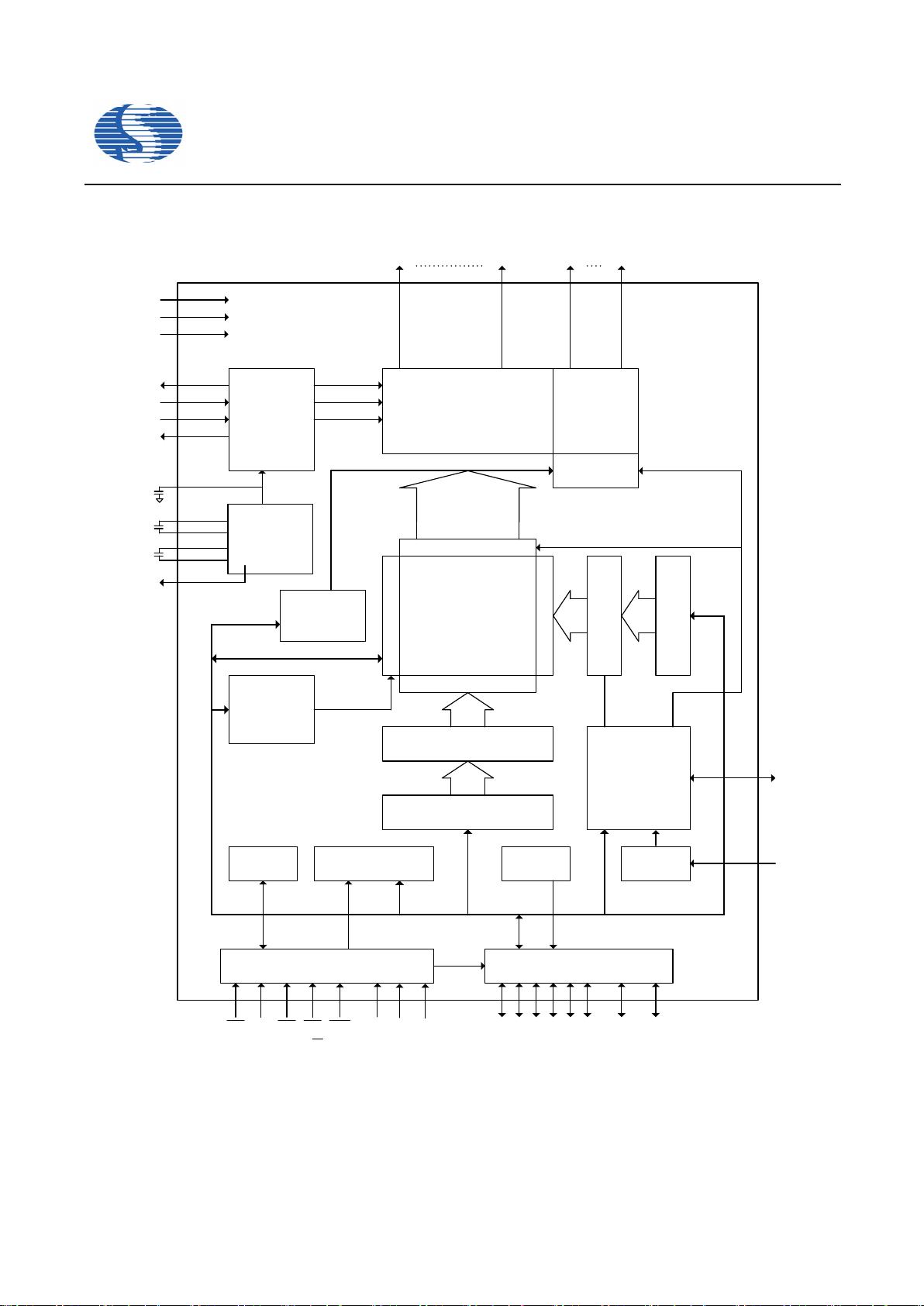
SH1106
132 X 64 Dot Matrix OLED/PLED
Segment/Common Driver with Controller
1 V2.3
Features
n Support maximum 132 X 64 dot matrix panel
n Embedded 132 X 64 bits SRAM
n Operating voltage:
- Logic voltage supply: VDD1 = 1.65V - 3.5V
- DC-DC voltage supply: VDD2 = 3.0V - 4.2V
- OLED Operating voltage supply:
External VPP supply = 6.4V - 14.0V
Internal VPP generator = 6.4V - 9.0V
n Maximum segment output current: 200mA
n Maximum common sink current: 27mA
n 8-bit 6800-series parallel interface, 8-bit 8080-series
parallel interface, 3-wire & 4-wire serial peripheral
interface, 400KHz fast I
2
C bus interface
n Programmable frame frequency and multiplexing ratio
n Row re-mapping and column re-mapping (ADC)
n Vertical scrolling
n On-chip oscillator
n Programmable Internal charge pump circuit output
n 256-step contrast control on monochrome passive OLED
panel
n Low power consumption
- Sleep mode: <5mA
- VDD1=0V,VDD2=3.0V – 4.2V: <5mA
- VDD1,2=0V,VPP=6.4V –14.0V: <5mA
n Wide range of operating temperatures: -40 to +85°C
n Available in COG form, thickness: 300mm
General Description
SH1106 is a single-chip CMOS OLED/PLED driver with controller for organic/polymer light emitting diode dot-matrix graphic
display system. SH1106 consists of 132 segments, 64 commons that can support a maximum display resolution of 132 X 64. It
is designed for Common Cathode type OLED panel.
SH1106 embeds with contrast control, display RAM oscillator and efficient DC-DC converter, which reduces the number of
external components and power consumption. SH1106 is suitable for a wide range of compact portable applications, such as
sub-display of mobile phone, calculator and MP3 player, etc.


剩余48页未读,继续阅读
资源评论


qxbzxx
- 粉丝: 0
- 资源: 12


最新资源
- 基于Python的图像阴影检测与去除源码(高分期末大作业项目).zip
- 基于C++/Qt实现的井字棋游戏
- 基于 Python 编程语言的 Web 框架Django
- Python和Flask实现的基于体检数据的城市公共健康可视分析系统源码+使用说明.zip
- 基于python实现的华为智慧工地-安全帽检测
- buck-boost_2023-12-16_12-12-13.eprj
- 后端开发关于数据库和API开发的介绍
- 机器学习和数据挖掘课程设计-米其林餐厅数据挖掘管理系统源码+使用文档说明.zip
- html html html展示我与ai的对化
- 数据结构课程设计-全国交通出行咨询模拟系统C语言实现源码.zip
资源上传下载、课程学习等过程中有任何疑问或建议,欢迎提出宝贵意见哦~我们会及时处理!
点击此处反馈


