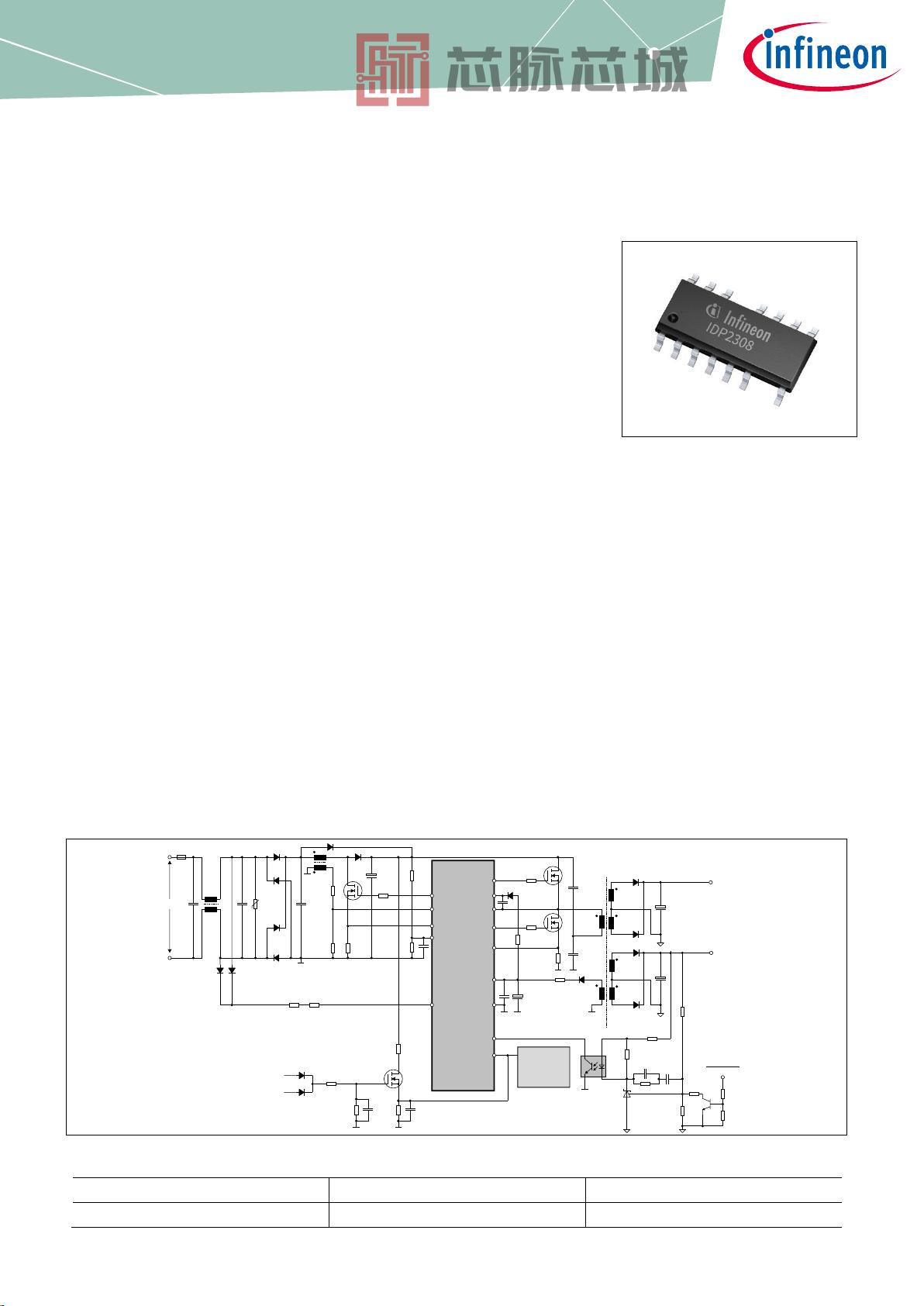
没有合适的资源?快使用搜索试试~ 我知道了~
IDP2308 英飞凌芯片 INFINEON 中文版规格书手册.pdf
需积分: 5 0 下载量 87 浏览量
2023-07-19
10:50:10
上传
评论
收藏 1.84MB PDF 举报
温馨提示
试读
38页
IDP2308 英飞凌芯片 INFINEON 中文版规格书手册
资源推荐
资源详情
资源评论
IDP2308
Digital Multi-Mode PFC + LLC Combo Controller
Product Highlights
Integrated 600V startup cell
Integrated floating driver based on coreless transformer technology
Digital multi-mode operation for higher efficiency curve
Supports low stand-by power by means of direct X-cap discharge function and
advanced burst mode control
Eliminates the auxiliary power supply by means of integrated startup cell and
burst mode
UART interface for communication and in-circuit configuration
Flexible design-in by means of one time programming capability for a wide range
of parameters
Description
The IDP2308 is a multi-mode PFC and LLC controller combined with a floating high side driver and a startup cell. A digital
engine provides advanced algorithms for multi-mode operation to support highest efficiency over the whole load range. A
comprehensive and configurable protection feature set is implemented. Only a minimum of external components are
required with the low pin count DSO-14 package. The integrated HV startup cell and advanced burst mode enable to achieve
low stand-by power. In addition a one-time-programming (OTP) unit is integrated to provide a wide set of configurable
parameters that help to ease the design in phase.
Features
Multi-mode PFC
Configurable PFC gate driver
Synchronous PFC and LLC burst mode control
Configurable non-linear LLC VCO curve
Configurable soft-start
V
AC
input voltage sensing and X cap discharge via HV pin
Applications
LCD-TV 75W ~ 300W
Generarl SMPS
Figure 1 Typical Application
Product Type
Package
Marking
IDP2308
PG-DSO-14
DP2308
HSGND
HSVCC
HSGD
GD1
CS1
IDP2308
GD0
VCC
GNDHV
VAC
ZCD
VS
CS0
Configuration
HBFB
Vout_2
MFIO
Vout_1
STANDBY
GD0
GD1
IDP2308
Digital Multi-Mode PFC + LLC Combo Controller
Datasheet 2 Rev. V2.3, 2018-08-13
Digital Multi-Mode PFC + LLC Combo Controller ............................................................................. 1
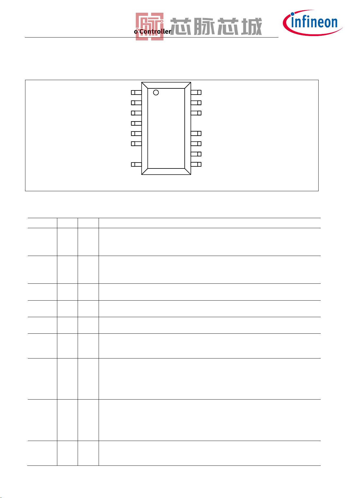
1 Pin Configuration and Description ................................................................................ 4
2 Representative Blockdiagram ...................................................................................... 6
3 Functional Description ................................................................................................ 7
3.1 Introduction ......................................................................................................................................... 7
3.2 Overview Controller Features ............................................................................................................. 7
3.3 Overview Controller Features ............................................................................................................. 7
3.3.1 System and Device overview ........................................................................................................ 8
3.3.1.1 Processor and memory operations ......................................................................................... 8
3.3.1.2 Communication interface ...................................................................................................... 10
3.3.1.3 Voltage and current sensors .................................................................................................. 10
3.3.2 IC Power Supply and High Voltage Startup Cell ......................................................................... 11
3.3.2.1 Direct AC input monitoring combined with VCC startup function ....................................... 11
3.3.2.2 X-cap discharge function via the integrated HV startup-cell ................................................ 12
3.3.3 Standby Mode with synchronous PFC-LLC burst operation ...................................................... 13
3.3.4 IC protection ................................................................................................................................ 13
3.3.4.1 Undervoltage lockout for VCC ............................................................................................... 13
3.3.4.2 Overvoltage protection for VCC ............................................................................................. 14
3.3.4.3 Over temperature protection ................................................................................................ 14
3.3.4.4 Auto Restart Mode .................................................................................................................. 14
3.3.5 AC detection ................................................................................................................................ 14
3.4 PFC Controller ................................................................................................................................... 14
3.4.1 PFC Softstart................................................................................................................................ 15
3.4.2 PFC Multi-mode operation .......................................................................................................... 15
3.4.3 PFC Protection ............................................................................................................................ 17
3.4.3.1 PFC Open Control Loop Protection (PFCOCLP) .................................................................... 17
3.4.3.2 PFC Inductor Over Current Protection (PFCOCP) ................................................................. 17
3.4.3.3 PFC Output Over Voltage Protection (PFCOVP) .................................................................... 17
3.4.3.4 PFC Output Redundant Over Voltage Protection (PFCROVP) .............................................. 17
3.4.3.5 PFC Output Under Voltage Protection (PFCUVP) .................................................................. 18
3.4.3.6 PFC Brownin Protection for AC Input Line (PFCBIP) ............................................................. 18
3.4.3.7 PFC Brownout Protection for AC Input Line (PFCBOP) ......................................................... 18
3.4.3.8 PFC Long Time Continuous Conduction Mode Protection (PFCCCMP) ............................... 18
3.5 Half-bridge LLC Controller ................................................................................................................ 19
3.5.1 LLC Softstart (Time Controlled Oscillator TCO) ......................................................................... 19
3.5.2 LLC Normal Operation (Voltage Controlled Oscillator VCO) ..................................................... 19
3.5.3 LLC Smooth Transition of Frequency Control from TCO to VCO ............................................... 21
3.5.4 LLC Half-bridge Protection ......................................................................................................... 21
3.5.4.1 LLC Open Control Loop Protection (LLCOCLP) ..................................................................... 21
3.5.4.2 LLC Over Load Protection (LLCOLP) ...................................................................................... 21
3.5.4.3 LLC Over Current Protection Level 1 (LLCOCP1) ................................................................... 21
3.5.4.4 LLC Over Current Protection Level 2 (LLCOCP2) ................................................................... 22
3.6 Operation Flow .................................................................................................................................. 22
3.6.1 IC Initialization ............................................................................................................................ 22
3.6.2 Operation Flow of the PFC Controller ........................................................................................ 23
3.6.3 Operation Flow of the Halfbridge LLC Controller ...................................................................... 24
3.7 Overview Protection Features .......................................................................................................... 25
IDP2308
Digital Multi-Mode PFC + LLC Combo Controller
Datasheet 3 Rev. V2.3, 2018-08-13
3.7.1 Undervoltage Lockout for VCC ................................................................................................... 25
3.7.2 Overvoltage Protection for VCC .................................................................................................. 26
3.7.3 Overtemperature Protection by means of internal Temperature Detection ............................ 26
3.8 Fixed and Configurable Parameters ................................................................................................. 27
3.8.1 Fixed Parameters ........................................................................................................................ 27
3.8.2 Configurable Parameters ............................................................................................................ 28
4 Electrical Characteristics ........................................................................................... 30
4.1 Absolute Maximum Ratings .............................................................................................................. 30
4.2 Package Characteristics .................................................................................................................... 31
4.3 Operating Conditions ........................................................................................................................ 31
4.4 DC Electrical Characteristics ............................................................................................................. 31
4.4.1 Power Supply Characteristics ..................................................................................................... 32
4.4.2 Characteristics of the MFIO Pin ................................................................................................... 32
4.4.3 Characteristics of the HBFB Pin .................................................................................................. 32
4.4.4 Characteristics of the Current Sense Inputs CSx ....................................................................... 33
4.4.5 Characteristics of the Zero Crossing Input ZCD ......................................................................... 33
4.4.6 Characteristics of the Gate Driver Pins GDx ............................................................................... 33
4.4.7 Characteristics of the High-Voltage Pin HV ................................................................................ 34
4.4.8 Characteristics of the VS Pin ....................................................................................................... 34
4.4.9 Characteristics of the HSGD Pin.................................................................................................. 34
5 Outline Dimensions and Marking ................................................................................ 36
5.1 Outline Dimensions ........................................................................................................................... 36
5.2 Marking .............................................................................................................................................. 36
Revision History ....................................................................................................................... 37
IDP2308
Digital Multi-Mode PFC + LLC Combo Controller
Datasheet 4 Rev. V2.3, 2018-08-13
1 Pin Configuration and Description
The pin configuration is shown in Figure 2 and Table 1. The Pin functions are described below.
Figure 2 Pin Configuration
Table 1 Pin Definitions and Functions
Symbol
Pin
Type
Function
GD0
(PFCGD)
1
O
Gate Driver Output 0 (PFC Gate Driver)
Output for directly driving the PFC PowerMOS. The default peak source current
capability is 156 mA and the peak sink current capability is 800 mA.
CS0
(PFCCS)
2
I
Current Sense 0 (PFC Current Sense)
Pin CS0 is connected to an external shunt resistor and the source of the PFC
PowerMOS.
VCC
3
P
Positive Voltage Supply
IC power supply
GND
4
G
Ground
IC ground
ZCD
5
I
Zero Crossing Detection
Pin ZCD is connected to the auxiliary winding of the PFC choke.
VS
6
I
Voltage Sensing
Pin VS is connected to a high ohmic resistor divider for directly sensing the bus
voltage.
HV
8
I
High Voltage Input
Pin HV is connected to the AC input via an external resistor and 2 diodes. There is
a 600 V HV startup-cell internally connected that is used for initial VCC charge. It
is also used to discharge the x-capacitors of the EMI network. Furthermore
sampled high voltage sensing is supported for brownin/brownout detection.
MFIO
9
I
MFIO
Pin MFIO provides a half duplex UART communication IO interface for parameter
configuration. It also can be used for PFC output redundant over voltage
protection. In that case it is recommended to use a BSS127 transistor as shown
in Figure 1 and the described in section 3.4.3.4.
HBFB
10
I
Half Bridge Feedback
Pin HBFB is connected to an optocoupler for the feedback path to control the
LLC switching frequency.
1
2
3
4
14
15
16
HSGND
GD0
HSVCC
VCC
HSGD
GND
5
6
8
10
11
12
HBFB
ZCD
CS1
GD1
HV
9
MFIO
VS
CS0
IDP2308
PG-DSO-14 (150mil)
IDP2308
Digital Multi-Mode PFC + LLC Combo Controller
Datasheet 5 Rev. V2.3, 2018-08-13
Symbol
Pin
Type
Function
CS1
(HBCS)
11
I
Current Sense 1 (Hallf Bridge current Sense)
Pin CS1 is connected to an external shunt resistor and the source of the
PowerMOS in the half-bridge stage.
GD1
(LSGD)
12
O
Gate Driver Output 1 (Half Bridge Low Side Gate Driver)
Output for directly driving the lowside PowerMOS in the half-bridge. The peak
source current capability is 120 mA and the peak sink current capability is 500
mA.
HSGND
14
G
High side Ground
Ground for floating high side driver
HSVCC
15
P
High side VCC
Power supply of the high side floating driver, supplied via bootstrap
HSGD
16
O
High side floating Gate Driver
Output for directly driving the high side PowerMOS in the half-bridge. The peak
source current capability is 0.52 A and the peak sink current capability is 1.3 A.
Refer to item 4.4.9 for more details.
剩余37页未读,继续阅读
资源评论
芯脉芯城
- 粉丝: 3
- 资源: 4031
上传资源 快速赚钱
- 我的内容管理 展开
- 我的资源 快来上传第一个资源
- 我的收益 登录查看自己的收益
- 我的积分 登录查看自己的积分
- 我的C币 登录后查看C币余额
- 我的收藏
- 我的下载
- 下载帮助
安全验证
文档复制为VIP权益,开通VIP直接复制
信息提交成功