没有合适的资源?快使用搜索试试~ 我知道了~
IRLR2908 INFINEON 英飞凌芯片 中文版规格书手册.pdf
需积分: 5 0 下载量 46 浏览量
2023-06-25
09:57:54
上传
评论
收藏 329KB PDF 举报
温馨提示
![preview](https://dl-preview.csdnimg.cn/87946070/0001-ecfb5c323ec01ac759895e35e816b321_thumbnail.jpeg)
![preview-icon](https://csdnimg.cn/release/downloadcmsfe/public/img/scale.ab9e0183.png)
试读
11页
IRLR2908 INFINEON 英飞凌芯片 中文版规格书手册
资源推荐
资源详情
资源评论
![pdf](https://img-home.csdnimg.cn/images/20210720083512.png)
![zip](https://img-home.csdnimg.cn/images/20210720083736.png)
![](https://csdnimg.cn/release/download_crawler_static/87946070/bg1.jpg)
10/01/10
www.irf.com 1
IRLR2908PbF
IRLU2908PbF
HEXFET
®
Power MOSFET
Description
This HEXFET ® Power MOSFET utilizes the latest processing techniques
to achieve extremely low on-resistance per silicon area. Additional features
of this HEXFET power MOSFET are a 175°C junction operating temperature,
low RθJC, fast switching speed and improved repetitive avalanche rating.
These features combine to make this design an extremely efficient and
reliable device for use in a wide variety of applications.
The D-Pak is designed for surface mounting using vapor phase, infrared,
or wave soldering techniques. The straight lead version (IRFU series) is
for through-hole mounting applications. Power dissipation levels up to 1.5
watts are possible in typical surface mount applications.
S
D
G
V
DSS
= 80V
R
DS(on)
= 28mΩ
I
D
= 30A
D-Pak
IRLR2908PbF
Features
l
Advanced Process Technology
l
Ultra Low On-Resistance
l
Dynamic dv/dt Rating
l
175°C Operating Temperature
l
Fast Switching
l
Repetitive Avalanche Allowed up to Tjmax
l
Lead-Free
I-Pak
IRLU2908PbF
Absolute Maximum Ratings
Parameter Units
I
D
@ T
C
= 25°C
Continuous Drain Current, V
GS
@ 10V (Silicon Limited)
A
I
D
@ T
C
= 100°C
Continuous Drain Current, V
GS
@ 10V (See Fig. 9)
I
D
@ T
C
= 25°C
Continuous Drain Current, V
GS
@ 10V
(Package Limited)
I
DM
Pulsed Drain Current
c
P
D
@T
C
= 25°C
Maximum Power Dissipation W
Linear Derating Factor W/°C
V
GS
Gate-to-Source Voltage V
E
AS
Single Pulse Avalanche Energy (Thermally Limited)
d
mJ
E
AS
(tested)
Sin
g
le Pulse Avalanche Ener
gy
Tested Value
i
I
AR
Avalanche Current
c
A
E
AR
Repetitive Avalanche Ener
gy
h
mJ
dv/dt
Peak Diode Recovery dv/dt
e
V/ns
T
J
Operating Junction and °C
T
STG
Storage Temperature Range
Soldering Temperature, for 10 seconds
Thermal Resistance
Parameter Typ. Max. Units
R
θJC
Junction-to-Case ––– 1.3 °C/W
R
θJA
Junction-to-Ambient (PCB Mount)
j
––– 40
R
θJA
Junction-to-Ambient ––– 110
120
0.77
± 16
180
250
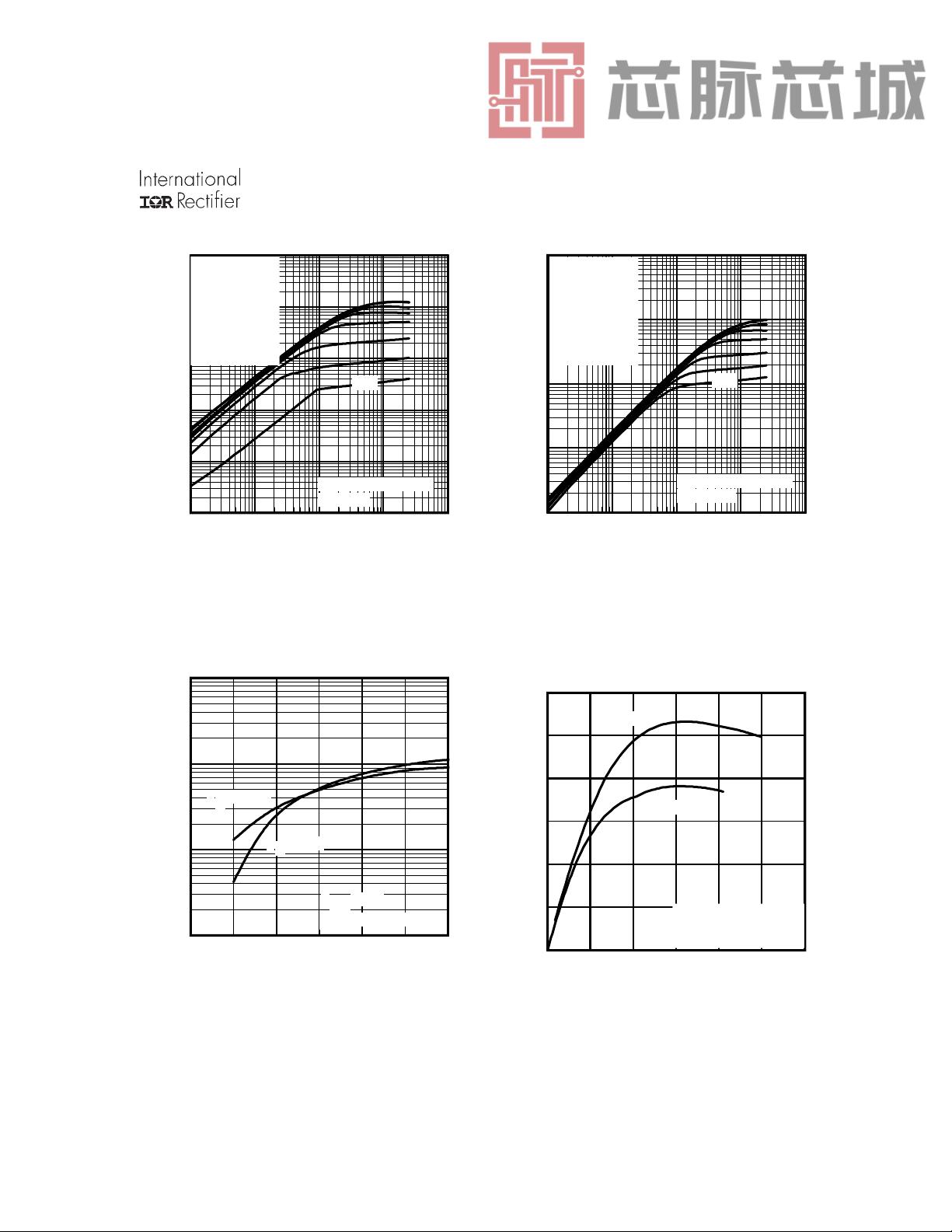
See Fig.12a,12b,15,16
Max.
39
28
150
30
300 (1.6mm from case )
-55 to + 175
2.3
PD - 95552B
![](https://csdnimg.cn/release/download_crawler_static/87946070/bg2.jpg)
IRLR/U2908PbF
2 www.irf.com
S
D
G
S
D
G
Notes through are on page 11
HEXFET
®
is a registered trademark of International Rectifier.
Static @ T
J
= 25°C (unless otherwise specified)
Parameter Min. Typ. Max. Units
V
(BR)DSS
Drain-to-Source Breakdown Voltage 80 ––– ––– V
∆ΒV
DSS
/
∆T
J
Breakdown Voltage Temp. Coefficient ––– 0.085 ––– V/°C
R
DS(on)
Static Drain-to-Source On-Resistance ––– 22.5 28
mΩ
––– 25 30
V
GS(th)
Gate Threshold Voltage 1.0 ––– 2.5 V
gfs Forward Transconductance 35 ––– ––– S
I
DSS
Drain-to-Source Leakage Current ––– ––– 20 µA
––– ––– 250
I
GSS
Gate-to-Source Forward Leakage ––– ––– 200 nA
Gate-to-Source Reverse Leakage ––– ––– -200
Q
g
Total Gate Charge ––– 22 33 nC
Q
gs
Gate-to-Source Charge ––– 6.0 9.1
Q
gd
Gate-to-Drain ("Miller") Charge ––– 11 17
t
d(on)
Turn-On Delay Time ––– 12 ––– ns
t
r
Rise Time –––95–––
t
d(off)
Turn-Off Delay Time ––– 36 –––
t
f
Fall Time –––55–––
L
D
Internal Drain Inductance ––– 4.5 ––– nH Between lead,
6mm (0.25in.)
L
S
Internal Source Inductance ––– 7.5 ––– from package
and center of die contact
C
iss
Input Capacitance ––– 1890 ––– pF
C
oss
Output Capacitance ––– 260 –––
C
rss
Reverse Transfer Capacitance ––– 35 –––
C
oss
Output Capacitance ––– 1920 –––
C
oss
Output Capacitance ––– 170 –––
C
oss
eff.
Effective Output Capacitance ––– 310 –––
Diode Characteristics
Parameter Min. Typ. Max. Units
I
S
Continuous Source Current ––– ––– 39
(Body Diode) A
I
SM
Pulsed Source Current ––– ––– 150
(Body Diode)
c
V
SD
Diode Forward Voltage ––– ––– 1.3 V
t
rr
Reverse Recovery Time ––– 75 110 ns
Q
rr
Reverse Recovery Charge ––– 210 310 nC
t
on
Forward Turn-On Time Intrinsic turn-on time is negligible (turn-on is dominated by LS+LD)
V
DS
= 64V
V
GS
= 4.5V
ƒ = 1.0MHz, See Fig. 5
V
GS
= 0V, V
DS
= 1.0V, ƒ = 1.0MHz
V
GS
= 4.5V
f
MOSFET symbol
V
GS
= 0V
V
DS
= 25V
V
GS
= 0V, V
DS
= 64V, ƒ = 1.0MHz
Conditions
V
GS
= 0V, V
DS
= 0V to 64V
T
J
= 25°C, I
F
= 23A, V
DD
= 25V
di/dt = 100A/µs
f
T
J
= 25°C, I
S
= 23A, V
GS
= 0V
f
showing the
integral reverse
p-n junction diode.
V
DS
= V
GS
, I
D
= 250µA
V
DS
= 80V, V
GS
= 0V
V
DS
= 80V, V
GS
= 0V, T
J
= 125°C
R
G
= 8.3Ω
I
D
= 23A
V
DS
= 25V, I
D
= 23A
V
DD
= 40V
I
D
= 23A
V
GS
= 16V
V
GS
= -16V
V
GS
= 4.5V, I
D
= 20A
f
Conditions
V
GS
= 0V, I
D
= 250µA
Reference to 25°C, I
D
= 1mA
V
GS
= 10V, I
D
= 23A
f
![](https://csdnimg.cn/release/download_crawler_static/87946070/bg3.jpg)
IRLR/U2908PbF
www.irf.com 3
Fig 2. Typical Output CharacteristicsFig 1. Typical Output Characteristics
Fig 3. Typical Transfer Characteristics
Fig 4. Typical Forward Transconductance
vs. Drain Current
0.01 0.1 1 10 100
V
DS
, Drain-to-Source Voltage (V)
0.01
0.1
1
10
100
1000
I
D
,
D
r
a
i
n
-
t
o
-
S
o
u
r
c
e
C
u
r
r
e
n
t
(
A
)
2.5V
20µs PULSE WIDTH
Tj = 25°C
VGS
TOP 15V
10V
4.5V
4.0V
3.5V
3.0V
2.7V
BOTTOM 2.5V
0.01 0.1 1 10 100
V
DS
, Drain-to-Source Voltage (V)
0.1
1
10
100
1000
I
D
,
D
r
a
i
n
-
t
o
-
S
o
u
r
c
e
C
u
r
r
e
n
t
(
A
)
2.5V
20µs PULSE WIDTH
Tj = 175°C
VGS
TOP 15V
10V
4.5V
4.0V
3.5V
3.0V
2.7V
BOTTOM 2.5V
0 10 20 30 40 50 60
I
D
, Drain-to-Source Current (A)
0
10
20
30
40
50
60
G
F
S
,
F
o
r
w
a
r
d
T
r
a
n
s
c
o
n
d
u
c
t
a
n
c
e
(
S
)
T
J
= 25°C
T
J
= 175°C
VDS = 10V
20µs PULSE WIDTH
2 3 4 5
V
GS
, Gate-to-Source Voltage (V)
1
10
100
1000
I
D
,
D
r
a
i
n
-
t
o
-
S
o
u
r
c
e
C
u
r
r
e
n
t
(
Α
)
T
J
= 25°C
T
J
= 175°C
V
DS
= 25V
20µs PULSE WIDTH
剩余10页未读,继续阅读
资源评论
![avatar-default](https://csdnimg.cn/release/downloadcmsfe/public/img/lazyLogo2.1882d7f4.png)
![avatar](https://profile-avatar.csdnimg.cn/default.jpg!1)
芯脉芯城
- 粉丝: 3
- 资源: 4031
上传资源 快速赚钱
我的内容管理 展开
我的资源 快来上传第一个资源
我的收益
登录查看自己的收益我的积分 登录查看自己的积分
我的C币 登录后查看C币余额
我的收藏
我的下载
下载帮助
![voice](https://csdnimg.cn/release/downloadcmsfe/public/img/voice.245cc511.png)
![center-task](https://csdnimg.cn/release/downloadcmsfe/public/img/center-task.c2eda91a.png)
安全验证
文档复制为VIP权益,开通VIP直接复制
![dialog-icon](https://csdnimg.cn/release/downloadcmsfe/public/img/green-success.6a4acb44.png)